Data sampling method and apparatus with alternating edge sampling phase detection for loop characteristic stabilization

Active Publication Date: 2008-08-05
LATTICE SEMICON CORP
View PDF4 Cites 54 Cited by
  • Summary
  • Abstract
  • Description
  • Claims
  • Application Information

AI Technical Summary

Benefits of technology

[0019]When the raw edge sampling clock of preferred embodiments of the invention is locked to the data transition edge, the edge sampling clock samples data with positive or negative offset from the data transition edge. In these embodiments, the AES PD of the invention has two sampling states: an UP state and a DOWN state. In the UP state, the edge sampling clock samples data with positive offset with respect to the data transition edge (i.e., at the left boundary of the dead zone, as shown in FIGS. 1(b) and 4(a)) and the data sampling clock also samples the data. In the DOWN state, the edge sampling cloc

Problems solved by technology

However, the loop characteristics of a CDR using such a binary PD are dependent on the jitter amplitude of the input data stream and the CDR might not be robust over a wide range of jitter amplitude.
The unstable gain (KPD) due to jitter variation, of a conventional CDR that includes a binary PD based on a 2× oversampling technique as described with reference to FIG. 1(a), results in unreliable CDR loo

Method used


Image

  • Data sampling method and apparatus with alternating edge sampling phase detection for loop characteristic stabilization
  • Data sampling method and apparatus with alternating edge sampling phase detection for loop characteristic stabilization
  • Data sampling method and apparatus with alternating edge sampling phase detection for loop characteristic stabilization

Examples


Embodiment Construction

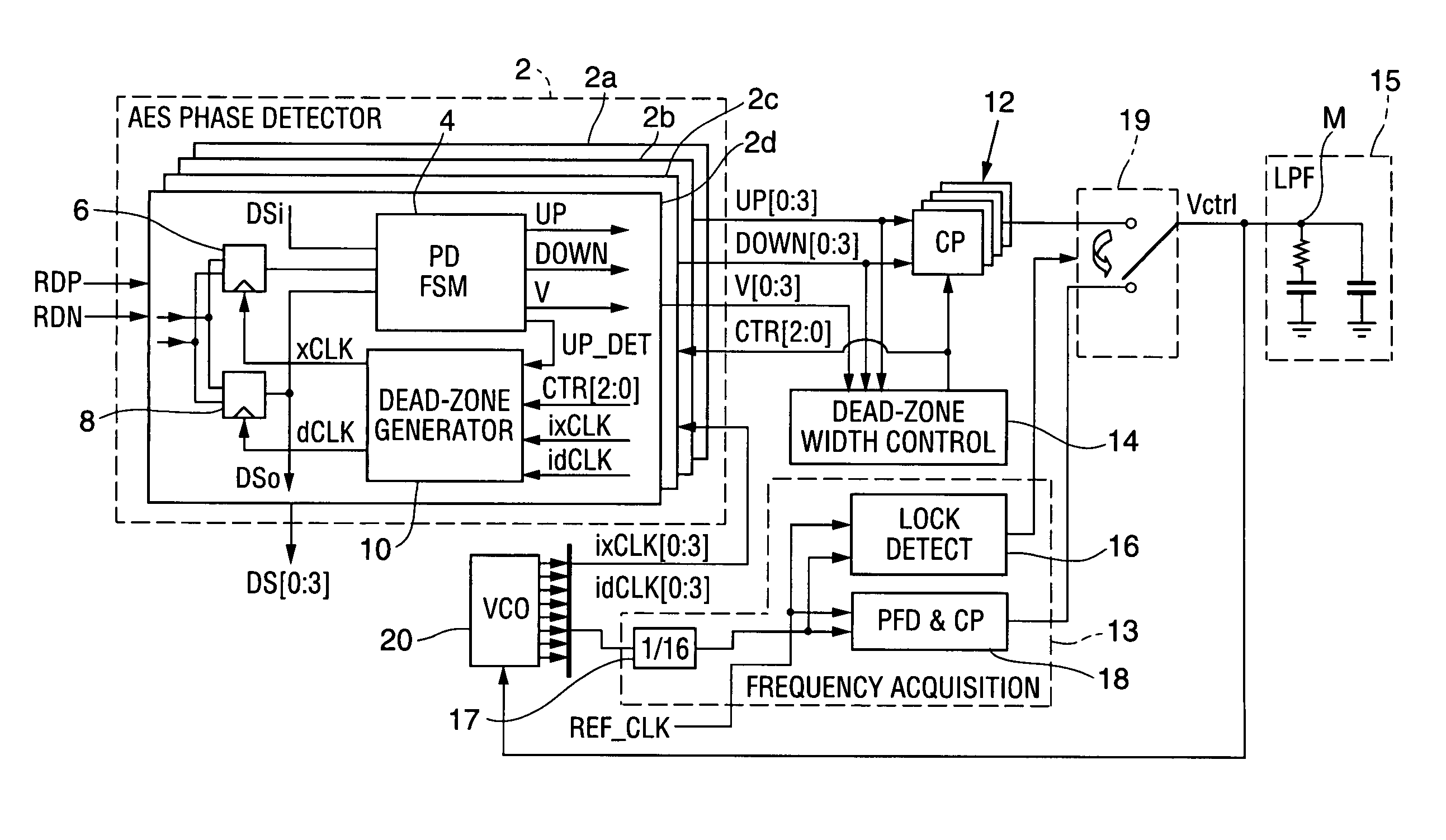
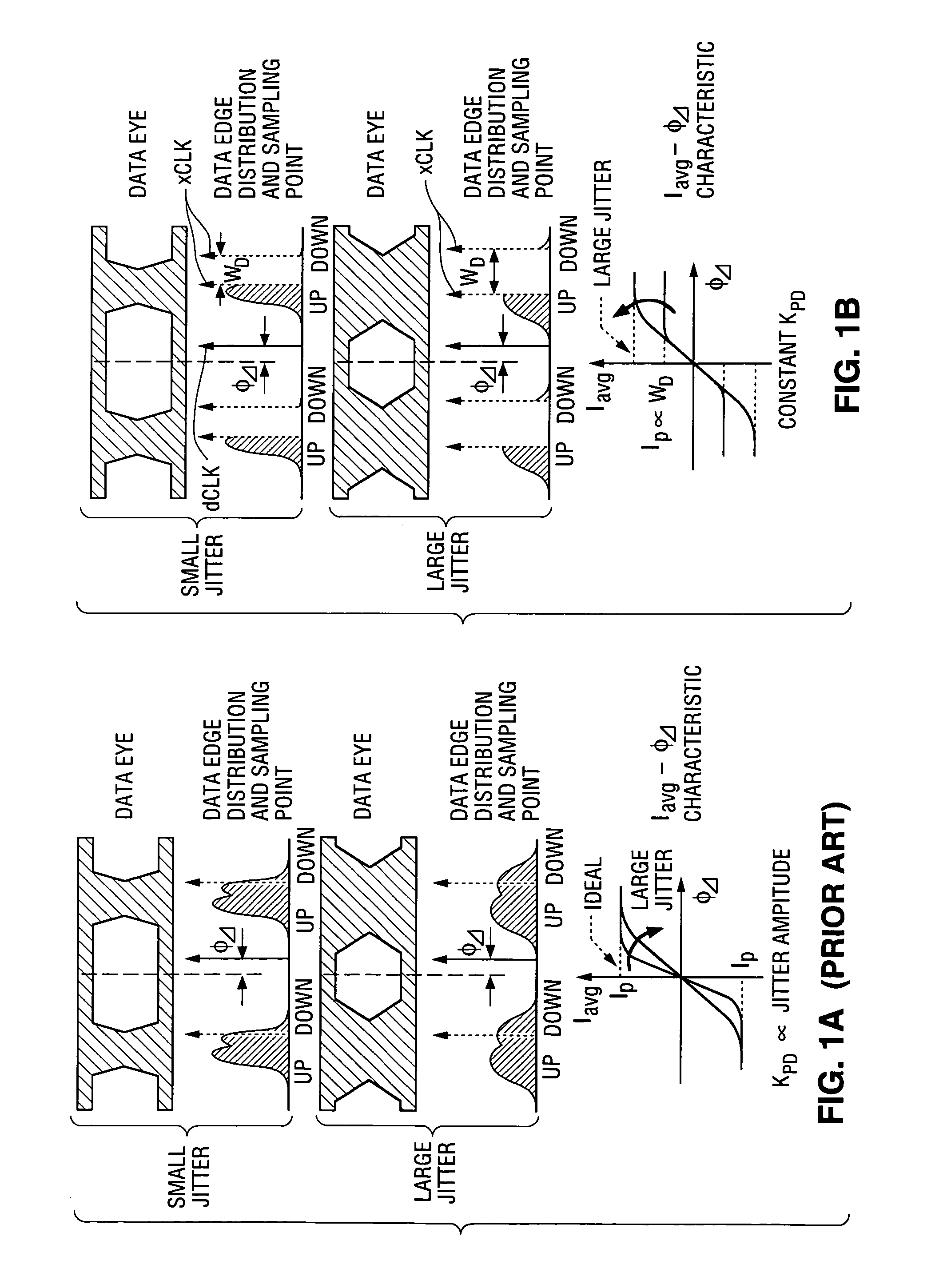
[0047]We sometimes refer to a circuit herein as a PD (e.g., an “alternating edge sampling PD”) when it includes not only a circuit that determines the phase error (φΔ) present between a sampling clock and data (being sampled by the clock), but also additional circuitry (e.g., data sampling circuitry). For example, alternating edge sampling phase detector (“AES PD”) 2 of FIG. 3(a) includes data sampling circuitry (e.g., circuit 8) as well as circuitry for generating signals (“up[0:3]” and “down[0:3]”) indicative of whether the data sampling clock employed by the data sampling circuitry leads or lags the data being sampled.

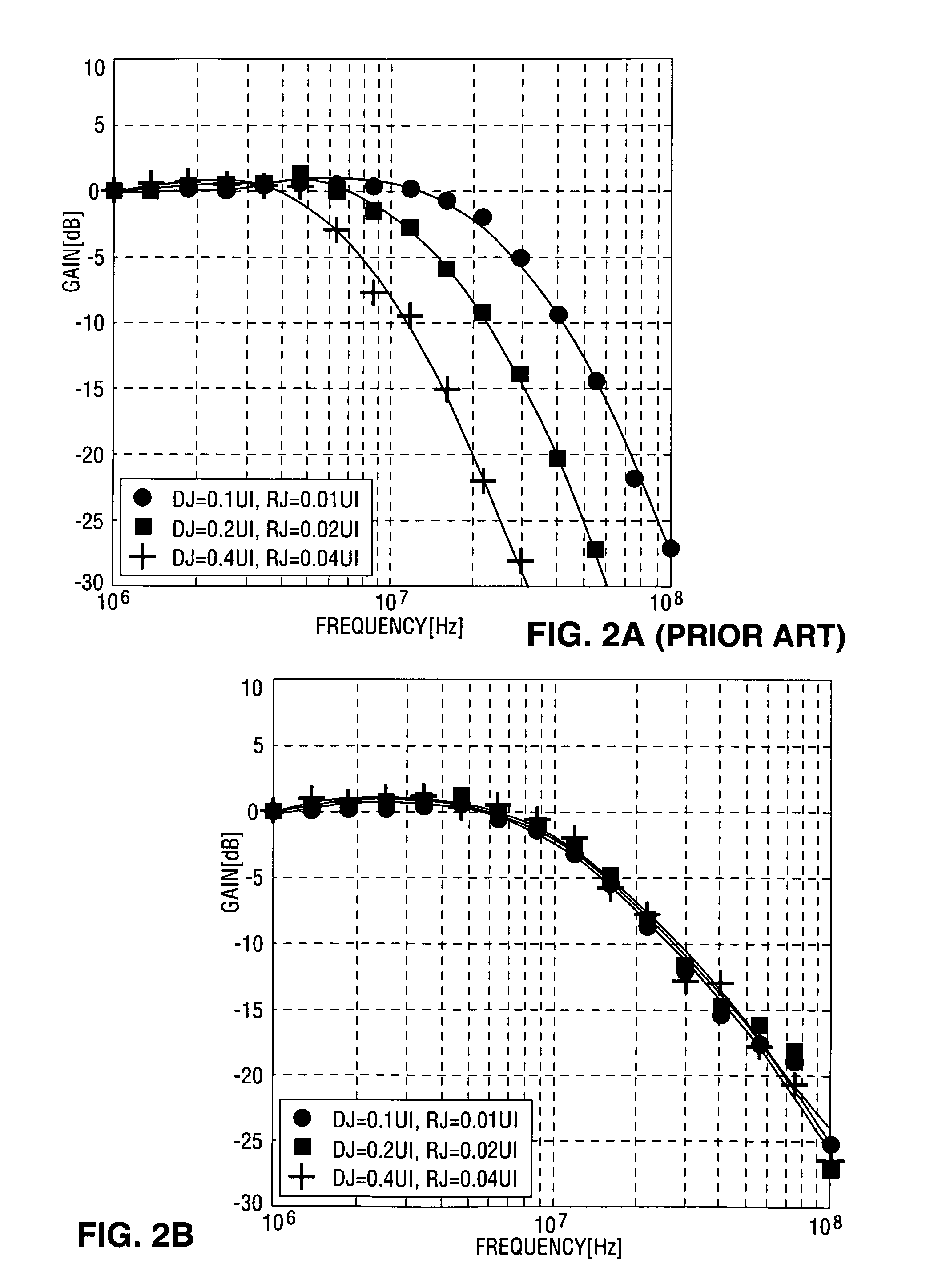
[0048]In a class of embodiments, the invention is a clock and data recovery device (CDR) that includes a binary phase detector (binary PD), employs a 2× oversampling technique, and is not subject to unstable gain (KPD) due to jitter variation. The inventive CDR includes a data loop configured to generate sampling clocks in response to a charge pump current IP having...


PUM


Abstract

A method and apparatus for 2× oversampling of data having jitter. In some embodiments, the invention is a clock and data recovery device including an alternating edge sampling binary phase detector, and which is configured to stabilize loop characteristics in various jitter environments and can be implemented with small hardware overhead. A transceiver that embodies the invention can be implemented as a CMOS integrated circuit using a 0.18 μm CMOS process, with the transceiver chip being capable of recovering data having a data rate of up to 11.5 Gbps from a signal received over a serial link, while consuming no more than 540 mW from 1.8V supply, and with a bit error rate of less than 10−12.

Description

CROSS-REFERENCE TO RELATED APPLICATION[0001]This application claims the benefit of U.S. Provisional Application No. 60 / 416,017, filed Oct. 4, 2002, entitled “A 2.5-10 GBPS CMOS TRANSCEIVER WITH ALTERNATING EDGE SAMPLING PHASE DETECTION FOR LOOP CHARACTERISTIC STABILIZATION.”FIELD OF THE INVENTION[0002]The invention pertains to clock and data recovery devices (CDRs), and to methods and circuitry for sampling data received over high speed links (e.g., high speed serial links).BACKGROUND OF THE INVENTION[0003]The term “receiver” is used herein in a broad sense to denote any device capable of receiving and decoding data that has been transmitted over a serial link or other link (and optionally also performing additional functions, which can include decrypting the received data and other operations related to decoding, reception, or decryption of the received data). For example, the term receiver can denote a transceiver that performs the functions of a transmitter as well as the functio...

Claims


Application Information

Patent Timeline
IPC IPC(8): H03D3/24
CPCH03L7/07H03L7/0805H03L7/0891H03L7/0995H04L7/033H03L7/107H03L7/10H04L7/0083H04L7/0091H03L7/113
Inventor LEE, BONG-JOONHWANG, MOON-SANGLEE, SANG-HYUNJEONG, DEOG-KYOON
Owner LATTICE SEMICON CORP
Why Eureka
Try Eureka