Leadless plastic chip carrier and method of fabricating same

a chip carrier and lead-less technology, applied in the direction of semiconductor devices, semiconductor/solid-state device details, electrical apparatus, etc., can solve the problems of limiting the package density of such prior art devices, and achieve the effects of shortening the wire bond length, reducing electrical impedance, and increasing thermal performan

Active Publication Date: 2008-08-12
UTAC HEADQUARTERS PTE LTD
View PDF68 Cites 26 Cited by
  • Summary
  • Abstract
  • Description
  • Claims
  • Application Information

AI Technical Summary

Benefits of technology

[0009]Advantageously, the heat sink provides a direct thermal path from the semiconductor die to the exterior of the package. The use of any thermally conductive but non-electrically conductive adhesive allows heat from the semiconductor die to be transferred from the exposed heat sink or through the adhesive to the contacts which are soldered to the motherboard. In embodiments of the present invention, a cavity is provided in the heat sink and the semiconductor die is mounted in the cavity. This feature allows for shorter wire bond lengths which results in decreased electrical impedance and increased thermal performance.
[0010]The integrated circuit package according to embodiments of the present invention is suitable for high power applications in which a motherboard has insufficient heat capacity to dissipate all heat from the semiconductor die. Further, the integrated circuit package is suitable in applications in which insufficient space is available on the motherboard for soldering a die attach pad. The integrated circuit package according to embodiments of the present invention provides for a heat sink that acts as a die attach pad on an opposite side of input / output contact leads. The heat sink (die attach pad) dimension can be standard for a particular package dimension, independent to the semiconductor die size and wire bond requirement, thereby providing a cost effective design that also provides for integration of power and ground signals in the package.

Problems solved by technology

The inner leads terminate in outer leads that are bent down to contact a mother board, thereby limiting the package density of such prior art devices.

Method used


Image

  • Leadless plastic chip carrier and method of fabricating same
  • Leadless plastic chip carrier and method of fabricating same
  • Leadless plastic chip carrier and method of fabricating same

Examples


Embodiment Construction

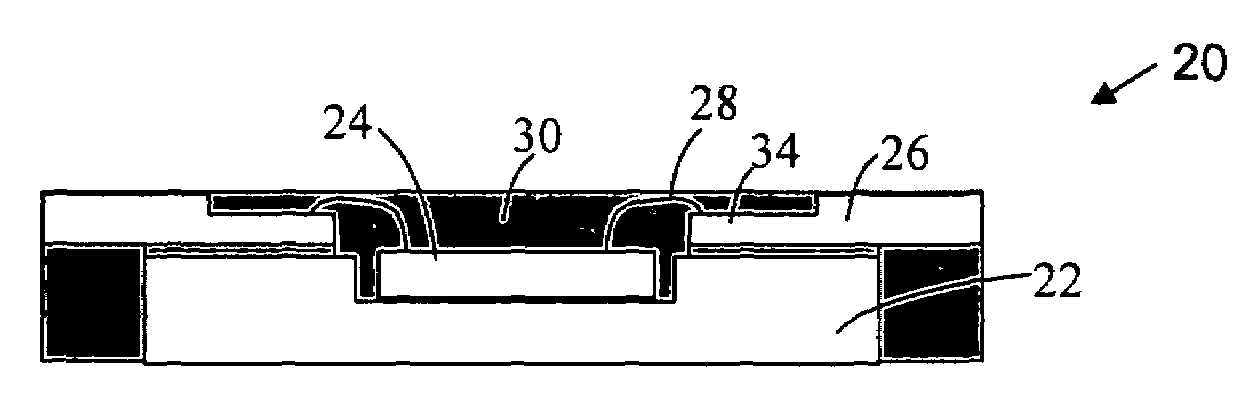
[0014]Reference is made to FIGS. 1 to 9 to describe a leadless plastic chip carrier (LPCC) according to one embodiment of the present invention, indicated generally by the numeral 20. The leadless plastic chip carrier 20 includes a heat sink 22 and a semiconductor die 24 is fixed to the heat sink 22 using an intermediary electrically non-conductive adhesive. A plurality of contacts 26 are fixed to the heat sink 22 such that the contacts 26 circumscribe the semiconductor die 24. A plurality of wire bonds 28 connect pads of the semiconductor die 24 to ones of the contacts 26 and a molding material 30 encapsulates the semiconductor die 24 and the wire bonds 28.

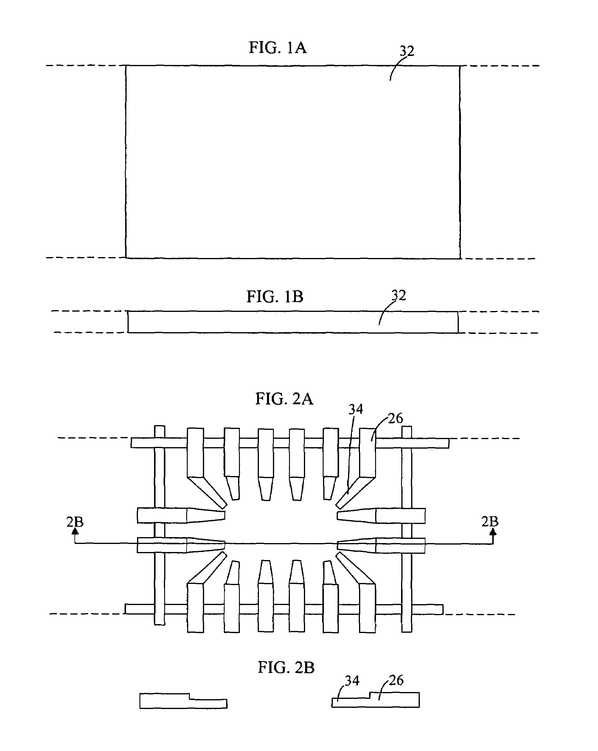
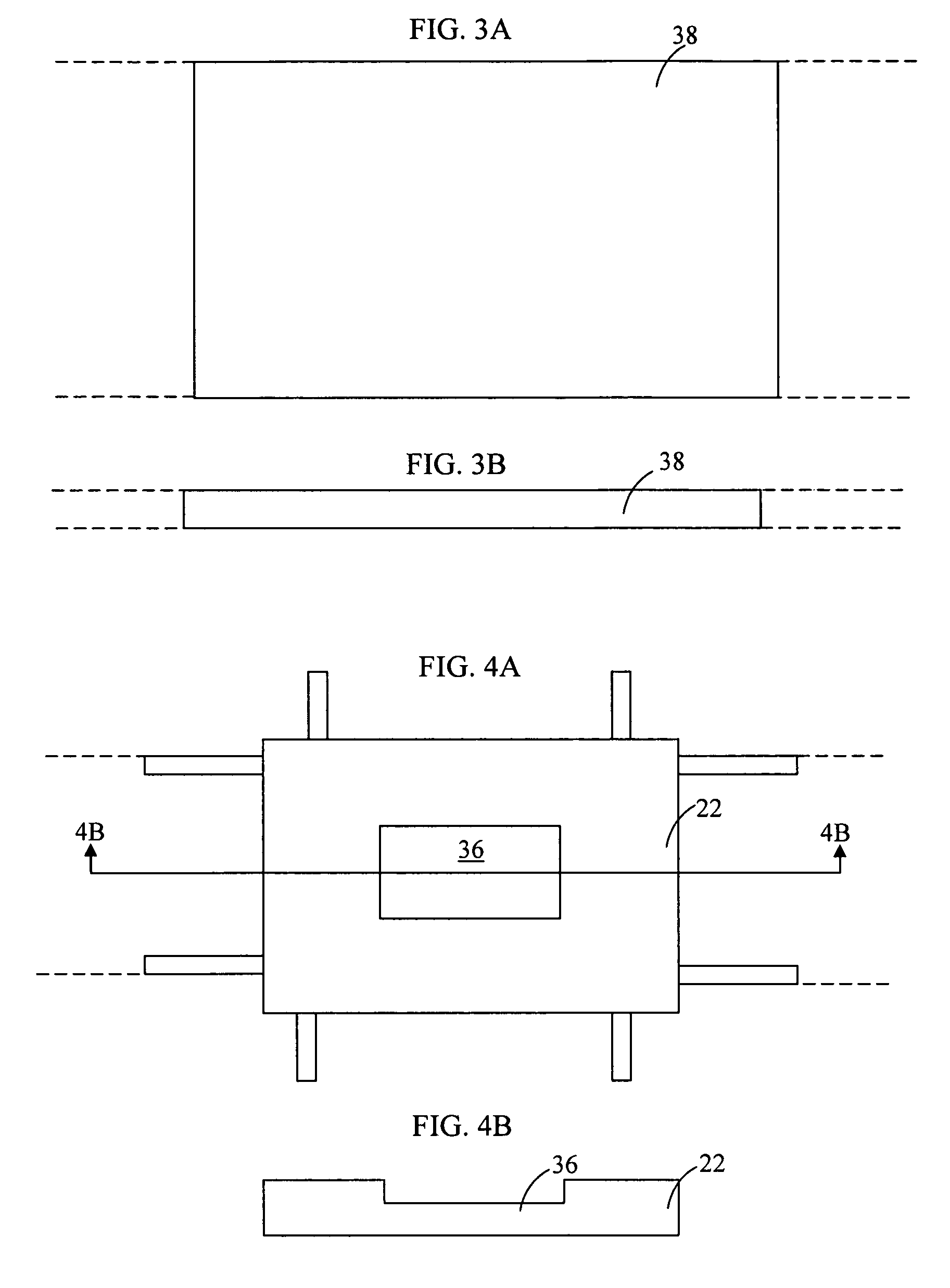
[0015]A process for manufacturing the LPCC package 20 will now be described in more detail. Referring to FIGS. 1A and 1B, there is provided an elevation view and a sectional side view, respectively, of a copper panel substrate 32 which forms the raw material of the leadframe strip. As discussed in greater detail in Applicants' ow...


PUM


Abstract

A process for fabricating a leadless plastic chip carrier includes providing a leadframe including a plurality of contacts circumscribing a void; fixing a heat sink to the contacts of the leadframe using an intermediate non-electrically conductive adhesive such that the heat sink spans the void; mounting a semiconductor die to the heat sink in the void; wire bonding ones of the contacts to the pads of the semiconductor die; encapsulating the semiconductor die and the wire bonds in a molding material and singulating the leadless plastic chip carrier.

Description

FIELD OF THE INVENTION[0001]The present invention relates in general to integrated circuit packaging, and more particularly to a leadless plastic chip carrier with features for improved thermal performance.BACKGROUND OF THE INVENTION[0002]According to well known prior art IC (integrated circuit) packaging methodologies, semiconductor dice are singulated and mounted using epoxy or other conventional means onto respective die attach pads of a leadframe strip. Traditional QFP (Quad Flat Pack) packages incorporate inner leads which function as lands for wire bonding the semiconductor die bond pads. These inner leads typically require mold locking features to ensure proper positioning of the leadframe strip during subsequent molding to encapsulate the package. The inner leads terminate in outer leads that are bent down to contact a mother board, thereby limiting the package density of such prior art devices.[0003]In order to overcome these and other disadvantages of the prior art, the Ap...

Claims


Application Information

Patent Timeline
Patent Type & Authority Patents(United States)
IPC IPC(8): H01L21/00
CPCH01L23/3107H01L23/49548H01L23/4334H01L24/48H01L24/45H01L2224/45144H01L2224/48091H01L2224/48247H01L2224/49171H01L2924/01046H01L2924/01078H01L2924/01079H01L2924/14H01L2924/3011H01L2924/01028H01L2224/73265H01L2924/07802H01L24/49H01L2924/00014H01L2924/00H01L2924/181H01L2924/00012
Inventor FAN, CHUN HOLIN, TSUI YEELAU, PING SHEUNG
Owner UTAC HEADQUARTERS PTE LTD
Why Eureka
Try Eureka