High electron mobility transistor (HEMT) structure with refractory gate metal

a high electron mobility, transistor technology, applied in the field of hemts, can solve the problems of reducing the height of the schottky barrier, increasing the current of the reverse gate, adverse effects on performance, etc., and achieve the effect of improving the long-term reliability of the inp hemt and superior performan

Active Publication Date: 2008-08-12
NORTHROP GRUMMAN SYST CORP
View PDF5 Cites 3 Cited by
  • Summary
  • Abstract
  • Description
  • Claims
  • Application Information

AI Technical Summary

Benefits of technology

[0005]The present invention developed from the recognition by one of the present inventors that the primary origin of performance degradation in InP HEMTs is the physical degradation of the Schottky junction formed between the gate metal electrode and the underlying semiconductor material in the HEMT structure. The present invention resides in a gate metal electrode that dramatically reduces the degree of Schottky junction degradation in testing at elevated temperatures and, therefore, correspondingly improves the long term reliability of the InP HEMT, whether implemented as a discrete device or in an integrated circuit, such as a MMIC.
[0007]In brief, without the refractory metal layer of the invention, titanium in the gate metal structure diffuses non-uniformly into the InAlAs barrier layer when the structure is exposed to elevated temperatures, producing some regions that are indium rich and others that are indium depleted. In terms of electrical characteristics of the gate junction, the interdiffusion of titanium results in an increase of reverse gate current / ideality factor and a decrease of Schottky barrier height, both of which have adverse effects on performance. With the refractory metal layer of the present invention in place, degradation of the Schottky barrier layer is minimized or eliminated and superior reliability performance is attained even at elevated performance.
[0008]Briefly, and in general terms, the indium phosphide (InP) high electron mobility transistor (HEMT) structure of the invention may be defined as comprising a semi-insulating substrate; an epitaxial structure formed on the substrate and comprising a semiconductor channel layer and an overlying semiconductor barrier layer; and a metal gate structure extending into the barrier layer and forming a Schottky junction with the barrier layer. In accordance with the invention, the metal gate structure comprises a first layer of a refractory metal in contact with the barrier layer, and additional layers of metal overlying the first layer. The first layer of the metal gate structure mitigates long-term degradation of the Schottky junction and improves long-term reliability of the HEMT structure.
[0010]It will be appreciated from the foregoing that the present invention represents a significant advance in InP HEMT technology. In particular, with a simple, but critical, change in gate metal structure the invention improves the long-term reliability of InP HEMTs without detracting from their superior performance, whether used as discrete devices or in integrated circuits. Other aspects and advantages of the invention will become apparent from the following more detailed description, taken in conjunction with the accompanying drawings.

Problems solved by technology

In terms of electrical characteristics of the gate junction, the interdiffusion of titanium results in an increase of reverse gate current / ideality factor and a decrease of Schottky barrier height, both of which have adverse effects on performance.

Method used


Image

  • High electron mobility transistor (HEMT) structure with refractory gate metal
  • High electron mobility transistor (HEMT) structure with refractory gate metal
  • High electron mobility transistor (HEMT) structure with refractory gate metal

Examples


Embodiment Construction

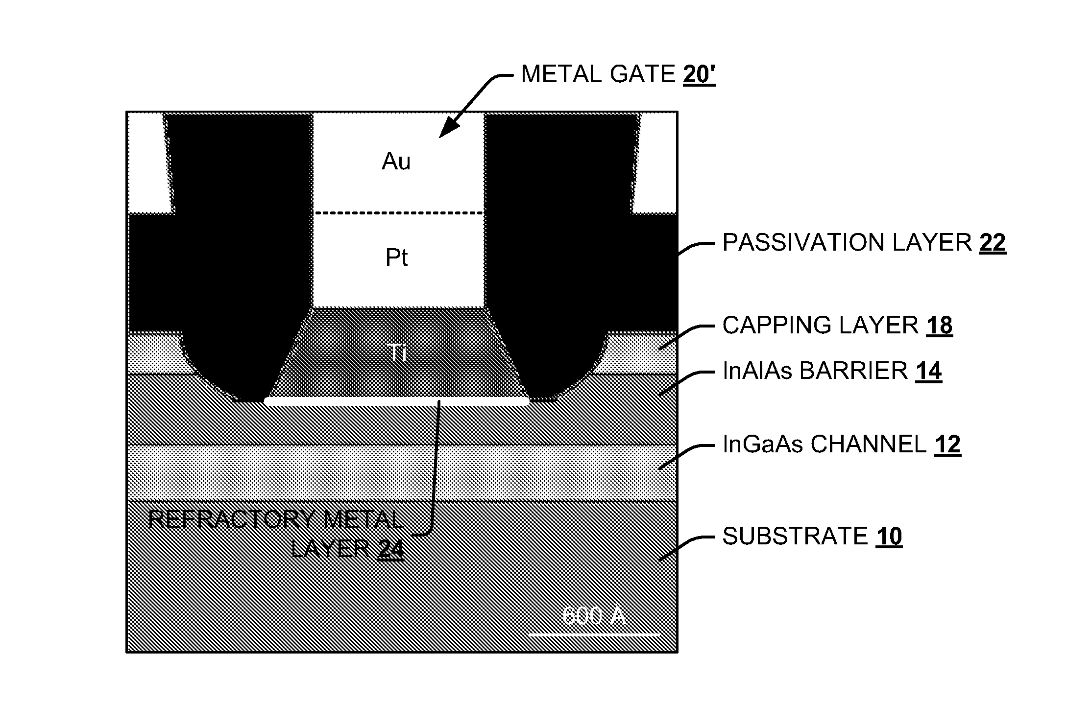
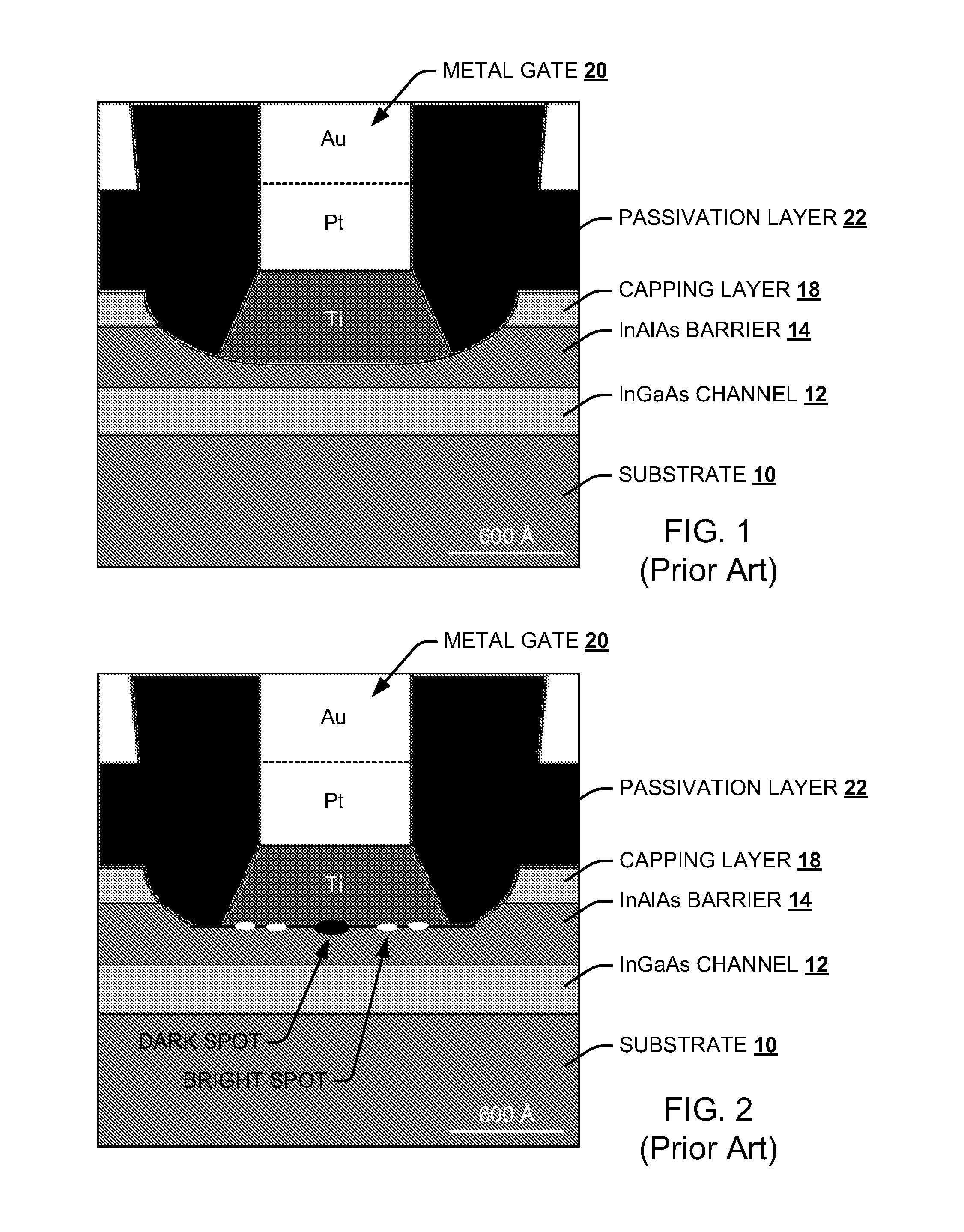
[0018]As shown in the drawings for purposes of illustration, the present invention is concerned with high electron mobility transistors (HEMTs) and, more particularly, with HEMTs employing indium phosphide (InP) and related materials. Prior to this invention InP HEMT devices, whether implemented as discrete devices or in integrated circuits such as microwave monolithic integrated circuits (MMICs), have typically included a gate metal structure consisting of three successive layers of titanium (Ti), platinum (Pt) and gold (Au). While it has been widely recognized that InP HEMTs have superior performance at microwave and millimeter wave frequencies, a known disadvantage of the devices is a potential to exhibit degradation in performance over long-term use.

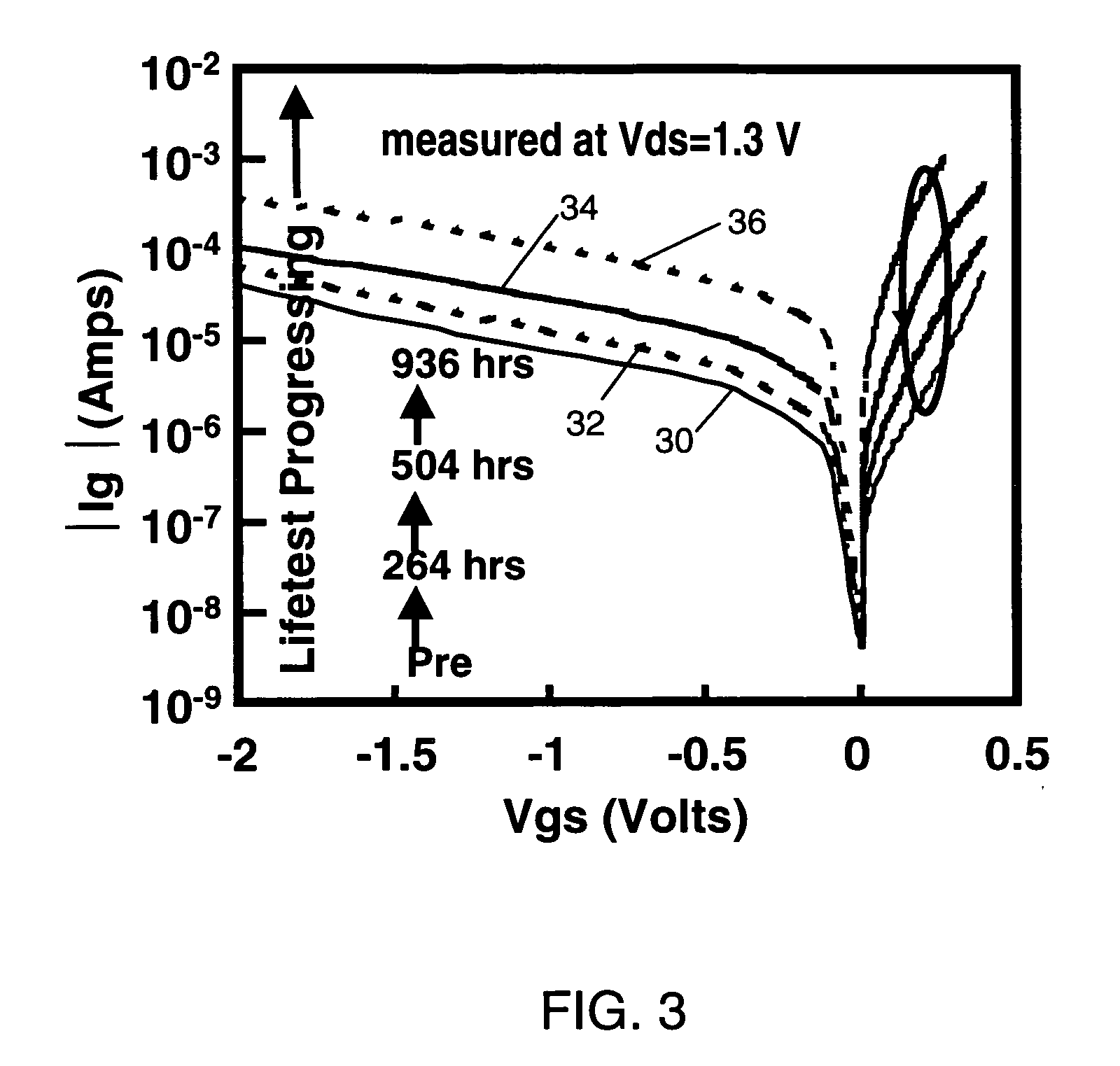
[0019]In the past, long-term performance degradation of InP HEMTs has been attributed a variety of degradation mechanisms. Recently, however, it has been shown by the present inventors that degradation of the Schottky junction betwee...


PUM

PropertyMeasurementUnit
thicknessaaaaaaaaaa
sizeaaaaaaaaaa
frequenciesaaaaaaaaaa

Abstract

An InP high electron mobility transistor (HEMT) structure in which a gate metal stack includes an additional thin layer of a refractory metal, such as molybdenum (Mo) or platinum (Pt) at a junction between the gate metal stack and a Schottky barrier layer in the HEMT structure. The refractory metal layer reduces or eliminates long-term degradation of the Schottky junction between the gate metal and the barrier layer, thereby dramatically improving long-term reliability of InP HEMTs, but without sacrifice in HEMT performance, whether used as a discrete device or in an integrated circuit.

Description

BACKGROUND OF THE INVENTION[0001]This invention relates generally to high electron mobility transistor (HEMT) structures and, more particularly, to HEMTs using indium phosphide (InP) and related materials. A HEMT is a type of field effect transistor (FET) in which current flow between two terminals, referred to as the source and drain terminals, is controlled by a voltage applied to a gate terminal. HEMTs are widely used in a variety of applications, but particularly as low noise amplifiers operating at microwave and millimeter wave frequencies. HEMTs may be implemented as discrete transistors or in integrated circuits, such as microwave monolithic integrated circuits (MMICs) in space, military and commercial applications.[0002]The present invention is particularly concerned with a known disadvantage of the InP HEMT, which includes, for example, a channel layer of indium gallium arsenide (InGaAs) and a barrier layer of indium aluminum arsenide (InAlAs) formed over an InP substrate. ...

Claims


Application Information

Patent Timeline
Patent Type & Authority Patents(United States)
IPC IPC(8): H01L31/00H01L21/28H01L29/80
CPCH01L29/7783H01L29/475H01L29/42316
Inventor CHOUG, YEONG-CHANGGRUNDBACHER, RONALDLIU, PO-HSINLEUNG, DENISE L.LAI, RICHARD
Owner NORTHROP GRUMMAN SYST CORP
Why Eureka
Try Eureka