Semiconductor integrated circuit and fabrication method thereof

a technology of integrated circuits and semiconductors, applied in the direction of transformers/inductance coils/windings/connections, inductances with magnetic cores, inductances, etc., can solve the problem of not being able to sufficiently miniaturize the semiconductor integrated circuit, and achieve the effect of improving the inductance and the q value of the inductor, reducing the area occupied by the inductor, and convenient magnetization

Inactive Publication Date: 2008-08-19
RENESAS ELECTRONICS CORP
View PDF19 Cites 12 Cited by
  • Summary
  • Abstract
  • Description
  • Claims
  • Application Information

AI Technical Summary

Benefits of technology

[0010]According to the present invention, the ferromagnetic core serves as a magnetic core of the inductor. Since the length of the ferromagnetic core in the direction perpendicular to the surface of the substrate, i.e., the height of the ferromagnetic core, is equal to or larger than the length thereof in the direction parallel to the surface of the substrate, i.e., the width thereof, the ferromagnetic core can be easily magnetized in a direction of a magnetic field induced by the inductor, i.e., in the direction perpendicular to the surface of the substrate. Thus, the inductance and the Q value of the inductor can be improved. Therefore, an area occupied by the inductor can be reduced and the size of the semiconductor integrated circuit can be reduced.
[0012]It is preferable that a plurality of ferromagnetic cores be provided. In this case, the width (the length in the direction parallel to the surface of the substrate) of each ferromagnetic core is reduced. Thus, it is possible to make the height (the length in the direction perpendicular to the surface of the substrate) of the ferromagnetic core larger than the width thereof without making the height excessively large.
[0014]It is preferable that the semiconductor integrated circuit of the present invention further comprise: a first metal layer provided in the region corresponding to the inner region of the inductor and below the ferromagnetic core; and a second metal layer provided to cover an upper surface and side faces of the ferromagnetic core. This can prevent diffusion of the material of the ferromagnetic core to other regions in the semiconductor integrated circuit.
[0015]It is preferable that an upper surface of the second metal layer be located in an upper level than an upper surface of the inductor. In this case, a current can flow through the upper surface of the inductor because of a skin effect, thus reducing a resistance value. As a result, the Q value of the inductor can be improved.
[0019]According to the present invention, the ferromagnetic core serves as a magnetic core of the inductor. In addition, the length of the ferromagnetic core in the direction perpendicular to the surface of the substrate is equal to or larger than the length thereof in the direction parallel to the surface of the substrate. Therefore, the ferromagnetic core can be easily magnetized in a direction of a magnetic field induced by the inductor, thus improving the inductance and the Q value of the inductor. As a result, an area occupied by the inductor can be reduced and the size of the semiconductor integrated circuit can be reduced.

Problems solved by technology

However, this conventional semiconductor integrated circuit has the following problem.
However, the aforementioned conventional techniques have the following problem.
Thus, it is not-possible to sufficiently miniaturize the semiconductor integrated circuit.

Method used


Image

  • Semiconductor integrated circuit and fabrication method thereof
  • Semiconductor integrated circuit and fabrication method thereof
  • Semiconductor integrated circuit and fabrication method thereof

Examples


first embodiment

[0030]Preferred embodiments of the present invention will be now described with reference to the accompanying drawings. the present invention will be described. FIG. 3 is a plan view of a semiconductor integrated circuit of the present embodiment, and FIGS. 4 and 5 are cross-sectional views of that semiconductor integrated circuit, taken along the line A-A and the line B-B in FIG. 3, respectively.

[0031]As shown in FIGS. 3 to 5, in the semiconductor integrated circuit of the present embodiment, a multilayer interconnection layer 1 is provided on a semiconductor substrate 50 that is formed of silicon, for example. The multilayer interconnection layer 1 is formed of a plurality of layers. On an insulating layer 2 that forms the uppermost layer of the multilayer interconnection layer 1, an inductor 3 is provided. The inductor 3 is a spiral inductor. The inductor 3 is formed of a single wiring 3a that is spirally arranged. The thickness of the insulating layer 2 is 1.5 μm, for example. W...

third embodiment

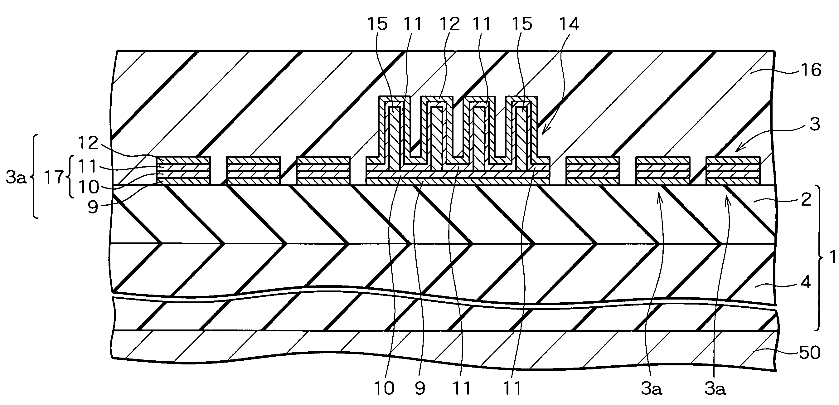
[0060]Then, as shown in FIGS. 10A to 10D, a TiW layer 9, a Cu layer 10, a ferromagnetic layer 15, a Cu layer 11, and a TiW layer 12 are formed on the insulating layer 2 in all areas in that order. The processes shown in FIGS. 10A to 10D are the same as those shown in FIGS. 9A to 9D in the third embodiment described above.

[0061]Next, as shown in FIG. 10E, a resist layer (not shown) is formed on the TiW layer 12. Then, using this resist layer as a mask, the TiW layer 9, the Cu layer 10, the Cu layer 11, and the TiW layer 12 are etched by wet etching, so that they are selectively removed and patterned. Wet etching of the Cu layers 10 and 11 can use SPM that is a mixture of sulfuric acid and hydrogen peroxide, while wet etching of the TiW layers 9 and 12 can use a hydrogen peroxide solution.

second embodiment

[0062]In this manner, a multilayer structure body 14 having a square shape is formed in a region corresponding to the inside of the inductor 3 in a plan view. The multilayer structure body 14 is formed of the TiW layer 9, the Cu layer 10, the ferromagnetic layer 15, the Cu layer 11, and the TiW layer 12. Then, an insulating layer 16 is formed of polyimide on the insulating layer 2 in all areas to embed the multilayer structure body 14. Thus, the semiconductor integrated circuit of the second embodiment can be fabricated.

[0063]The shape of the ferromagnetic core 15 is columnar, for example, as described in the first to fourth embodiments. However, the present invention is not limited thereto. The ferromagnetic core 15 may have any shape as,long as its height is equal to or larger than its width.


PUM

PropertyMeasurementUnit
thicknessaaaaaaaaaa
inductanceaaaaaaaaaa
thicknessaaaaaaaaaa

Abstract

A multilayer interconnection layer is provided on a semiconductor substrate. An inductor is provided on an insulating layer that forms the uppermost layer of the multilayer interconnection layer. The inductor is formed by spirally arranging a single wiring. On the insulating layer, a multilayer structure body is provided in an inner region of the inductor. In the multilayer structure body, a plurality of ferromagnetic cores formed of Ni are arranged in a matrix. The height of each ferromagnetic core is equal to or larger than the width thereof.

Description

BACKGROUND OF THE INVENTION[0001]1. Field of the Invention[0002]The present invention relates to a semiconductor integrated circuit including an inductor and a fabrication method thereof.[0003]2. Description of the Related Art[0004]FIG. 1 is a plan view of a conventional semiconductor integrated circuit, and FIG. 2 is a cross-sectional view thereof, taken along the line E-E in FIG. 1. As shown in FIGS. 1 and 2, in this conventional semiconductor integrated circuit, a multilayer interconnection layer 101 is provided on a semiconductor substrate (not shown). In the uppermost layer 102 of the multilayer interconnection layer 101, an inductor 103 is provided. The inductor 103 is a spiral inductor. In other words, on an insulating layer 104 formed of SiO2 in the multilayer interconnection layer 101, the inductor 103 is provided. The inductor 103 is formed by a single wiring that is spirally arranged. In addition, an insulating layer 105 formed of SiO2 is provided to cover the inductor 10...

Claims


Application Information

Patent Timeline
Patent Type & Authority Patents(United States)
IPC IPC(8): H01F5/00H01F41/04H01F17/00H01F17/04H01L21/02H01L21/3205H01L21/822H01L23/52H01L23/522H01L27/04
CPCH01L23/5227H01L28/10H01F17/0006H01F41/046H01L2924/0002H01L2924/3011H01L2924/00
Inventor FURUMIYA, MASAYUKIYAMAMOTO, RYOTA
Owner RENESAS ELECTRONICS CORP
Why Eureka
Try Eureka