TFT LCD and fabricating method thereof having particular reflection bumps with stacked structure

a technology of stacked structure and reflection bumps, which is applied in the direction of instruments, non-linear optics, optics, etc., can solve the problems of reducing light scattering efficiency, high complexity and manufacturing cost, and the method costs much more than the transflective lcd without bumps, so as to achieve the effect of reducing manufacturing cost and time, and avoiding reflection and scattering performan

Inactive Publication Date: 2008-09-02
INNOCOM TECH CHENZHEN +1
View PDF7 Cites 9 Cited by
  • Summary
  • Abstract
  • Description
  • Claims
  • Application Information

AI Technical Summary

Benefits of technology

[0010]It is therefore a primary objective of the claimed invention to provide a method for fabricating a TFT LCD which forms a plurality of bumps in each subpixel and TFT at the same time, so that the fabrication cost can be reduced and the above-mentioned problem can be solved.
[0013]It is an advantage of the claimed invention that the stacked layers of the reflection bumps are formed together with the gates, the semiconductor channels, the sources, and drains. Therefore, when fabricating a reflective LCD, at least a photomask, a photolithography process, and an etching process can be omitted in contrast to the prior art. On the other hand, when the claimed invention method is applied to fabricating a transflective LCD, at least two photomasks, two photolithography processes, and two etching process can be omitted in contrast to the prior art. Accordingly, fabrication cost and time can be greatly saved. In addition, the claimed invention method is easily able to change the area of each stacked layer of the reflection bumps to adjust the convex angles of the reflection bumps according to various requirements and design considerations of different LCDs so that the roughness of reflective pattern layer surface can be adjusted to meet preferable reflection and scattering performance requirements. Therefore, the claimed invention can be applied to both reflective LCDs and transflective LCDs.

Problems solved by technology

Therefore, the complexity and cost of manufacture is high.
Accordingly, this method costs much more than that of transflective LCDs without bumps, which have the disadvantage of lower light scattering efficiency.
Thus, how to fabricate a reflective LCD or a transflective LCD with improved light reflection efficiency but with lower manufacturing cost remains an important issue for manufacturers.

Method used


Image

  • TFT LCD and fabricating method thereof having particular reflection bumps with stacked structure
  • TFT LCD and fabricating method thereof having particular reflection bumps with stacked structure
  • TFT LCD and fabricating method thereof having particular reflection bumps with stacked structure

Examples


first embodiment

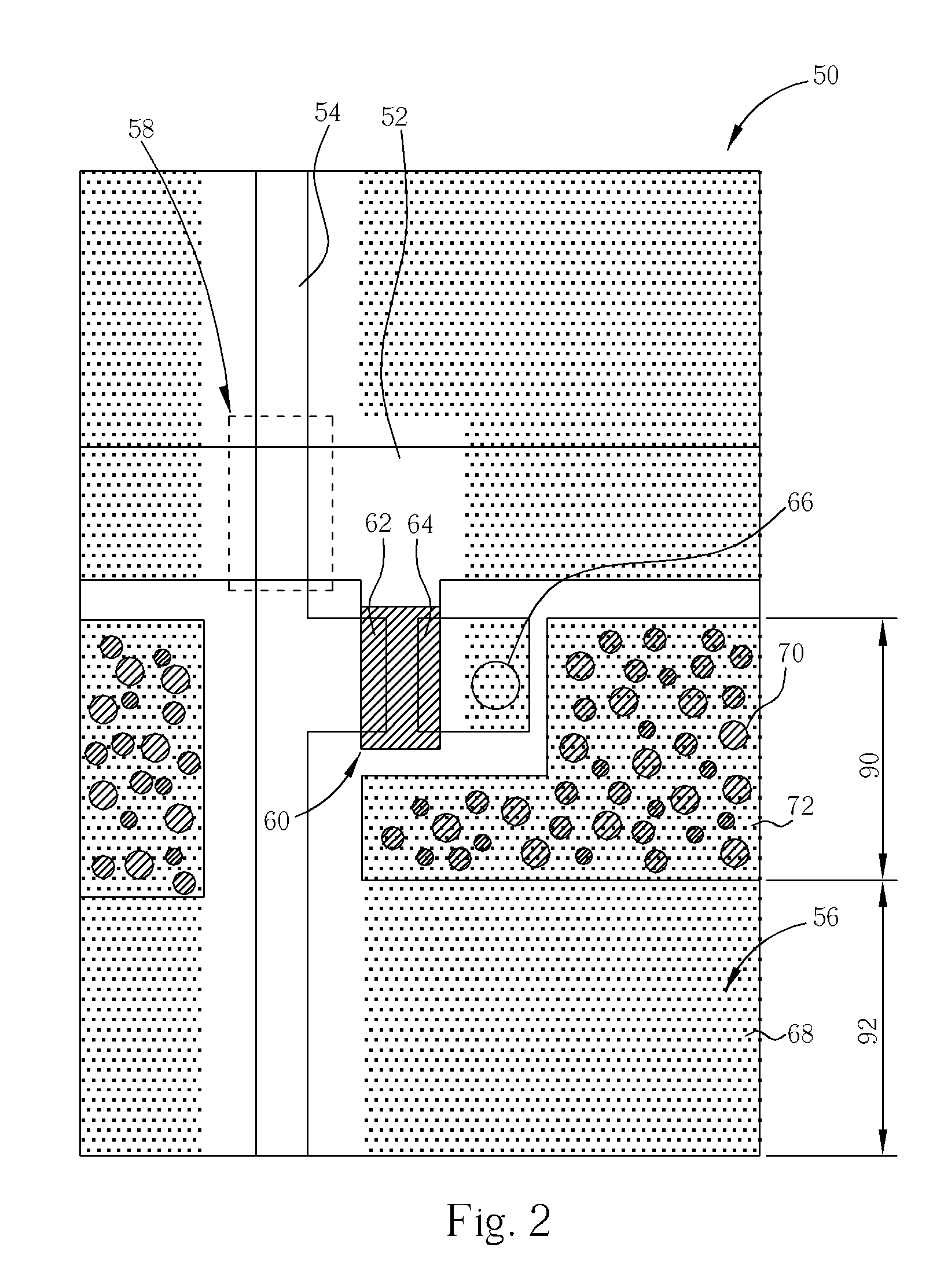
[0021]Please refer to FIGS. 2-6. FIG. 2 is a top view of a portion of a TFT LCD 50 according to the present invention, while FIGS. 3-6 are schematic diagrams of the fabricating process of the TFT LCD 50 shown in FIG. 2. In this embodiment, the TFT LCD 50 is a transflective LCD. As shown in FIG. 2, the TFT LCD 50 comprises a plurality of scan lines 52 and a plurality of data lines 54 (please note only one scan line 52 and one data line 54 is shown in FIG. 2). The scan lines 52 and the data lines 54 are arranged perpendicularly to define pluralities of subpixels 56, wherein the scan lines 52 and the data lines 54 are formed in different planes and cross perpendicularly in each cross over region 58. The TFT LCD 50 further comprises a plurality of TFTs 60, where each TFT 60 is positioned in a subpixel 56. The source 62 of each TFT 60 is electrically connected to a data line 54, and the drain 64 is electrically connected to a pixel electrode 68 through a via hole 66 in each subpixel56. E...

third embodiment

[0031]Please refer to FIG. 9. FIG. 9 is a schematic diagram of a portion of a TFT LCD 150 according to the present invention. The TFT LCD 150 is a reflective LCD, comprising a plurality of scan lines 152 and a plurality of data lines 154 arranged perpendicular to each other and crossing in a plurality of cross over regions 158, which divide the display area of the TFT LCD 150 into a plurality of subpixels 156. Each subpixel 156 includes a TFT 160 and a pixel electrode 168. Each TFT 160 comprises a source 162 and drain 164, and the source 162 is electrically connected to a corresponding data line 154, whereas the drain 164 is electrically connected to the pixel electrodes 168 through a via hole 166. The TFT LCD 150 is a reflective LCD, so the pixel electrodes 168 are formed with reflective materials, preferably with metal materials, such as aluminum, chromium, titanium, tungsten, tantalum, alloy, or a combination of materials mentioned above. In addition, a plurality of reflection bu...

fourth embodiment

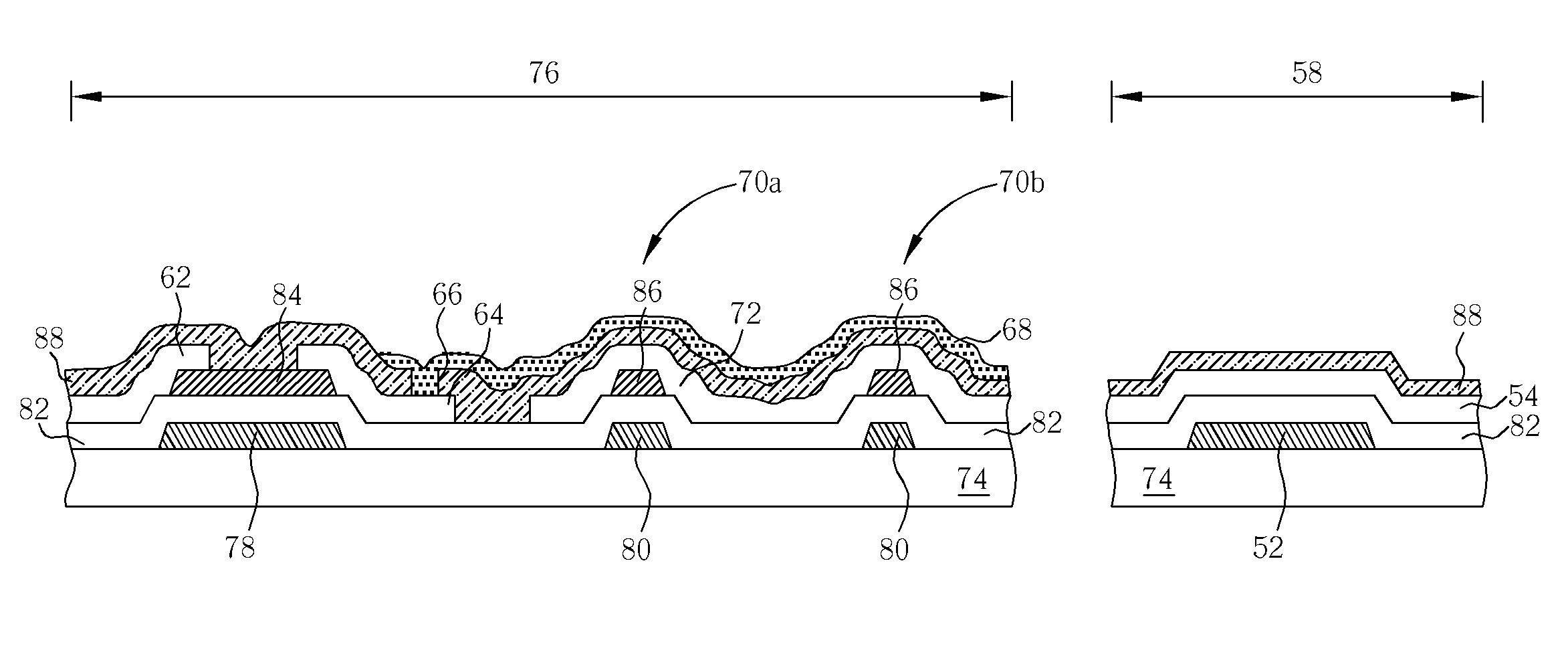
[0034]Please refer to FIG. 11. FIG. 11 is a section view of a portion of a TFT LCD 150 according to the present invention, wherein the TFT LCD 150 is a reflective LCD. For illustration purposes, the numeral given to each element is the same as that in FIG. 10. In this embodiment, each reflection bump 170 is a stacked structure comprising a gate insulating layer 182, a bottom bump pattern 180, a top bump pattern 186, a passivation layer 188, and a reflective pattern layer 172. The bottom bump patterns 180 are formed together with the semiconductor channels 184 of TFTs 160. This means the semiconductor layer is etched to define the patterns of the semiconductor channels 184 and define the bottom bump patterns 180 simultaneously. On the other hand, the top bump patterns 186, the source 162 and the drain 164 of each TFT 160 are formed at the same time, so that the top bump patterns 186 are defined on the bottom bump patterns 180 in order to make the bottom bump patterns 180 and the top ...


PUM

PropertyMeasurementUnit
reflectionaaaaaaaaaa
sizeaaaaaaaaaa
sizesaaaaaaaaaa

Abstract

A TFT LCD that can reflect incident lights and a fabrication method thereof are disclosed. The TFT LCD comprises plural bumps in each subpixel. Each bump has a stacked structure, which is formed with the TFTs simultaneously. The bumps can reflect and scatter incident light so as to promote the reflection performance of the TFT LCD.

Description

BACKGROUND OF INVENTION[0001]1. Field of the Invention[0002]The invention relates to a thin film transistor (TFT) liquid crystal display (LCD), and more particularly, to a reflective TFT LCD or a transflective TFT LCD.[0003]2. Description of the Prior Art[0004]As technology of electronic products develops, human-machine interfaces such as displays are demanded for higher quality. Thin film transistor (TFT) Liquid crystal displays (LCDs) are characterized by portability, low power consumption and lack of radiation pollution, and thus are popularly used in various portable information products such as notebooks, personal digital assistants (PDAs), digital cameras, mobile phones et cetera. LCDs require external light sources to display images. Depending on the type of external source, LCDs can be divided into reflective LCDs, which use ambient lights, transmissive LCDs, which use backlight modules, and transflective LCDs, which use both ambient lights and backlight modules.[0005]In gen...

Claims


Application Information

Patent Timeline
Patent Type & Authority Patents(United States)
IPC IPC(8): G02F1/1335G02F1/136
CPCG02F1/133553G02F1/136227G02F2203/09G02F2201/123
Inventor LEE, HSIN-TA
Owner INNOCOM TECH CHENZHEN
Why Eureka
Try Eureka