Low temperature process to produce low-K dielectrics with low stress by plasma-enhanced chemical vapor deposition (PECVD)

a technology of plasma-enhanced chemical vapor deposition and low-temperature process, which is applied in the direction of plasma technique, semiconductor/solid-state device details, coatings, etc., can solve the problems of increasing parasitic capacitance between devices, reducing the response time of devices, and damage to device structures, etc., to achieve the effect of reducing film stress

Inactive Publication Date: 2008-09-09
APPLIED MATERIALS INC
View PDF47 Cites 29 Cited by
  • Summary
  • Abstract
  • Description
  • Claims
  • Application Information

AI Technical Summary

Benefits of technology

[0011]Low K dielectric films exhibiting a low tensile stress of less than about 20 MPa may be formed utilizing various techniques in accordance with the present invention. In one embodiment, carbon-containing silicon oxide films are formed by plasma-assisted chemical vapor deposition at low temperatures (300° C. or less). In accordance with another embodiment, as-deposited carbon containing silicon oxide films incorporate a porogen whose subsequent liberation reduces film stress.

Problems solved by technology

The high temperatures at which some thermal CVD processes operate can damage device structures having layers previously formed on the substrate.
However, the barrier / liner layers typically have dielectric constants that are greater than about 2.5, and the high dielectric constants result in a combined insulator that may not significantly reduce the dielectric constant.
Additionally, the smaller device geometries result in an increase in parasitic capacitance between devices.
Parasitic capacitance between metal interconnects on the same or adjacent layers in the circuit can result in crosstalk between the metal lines or interconnects and / or resistance-capacitance (RC) delay, thereby reducing the response time of the device and degrading the overall performance of the device.
Increasing the thickness of the dielectric materials, however, does not address parasitic capacitance within the same metallized layer or plane.

Method used


Image

  • Low temperature process to produce low-K dielectrics with low stress by plasma-enhanced chemical vapor deposition (PECVD)
  • Low temperature process to produce low-K dielectrics with low stress by plasma-enhanced chemical vapor deposition (PECVD)
  • Low temperature process to produce low-K dielectrics with low stress by plasma-enhanced chemical vapor deposition (PECVD)

Examples


examples

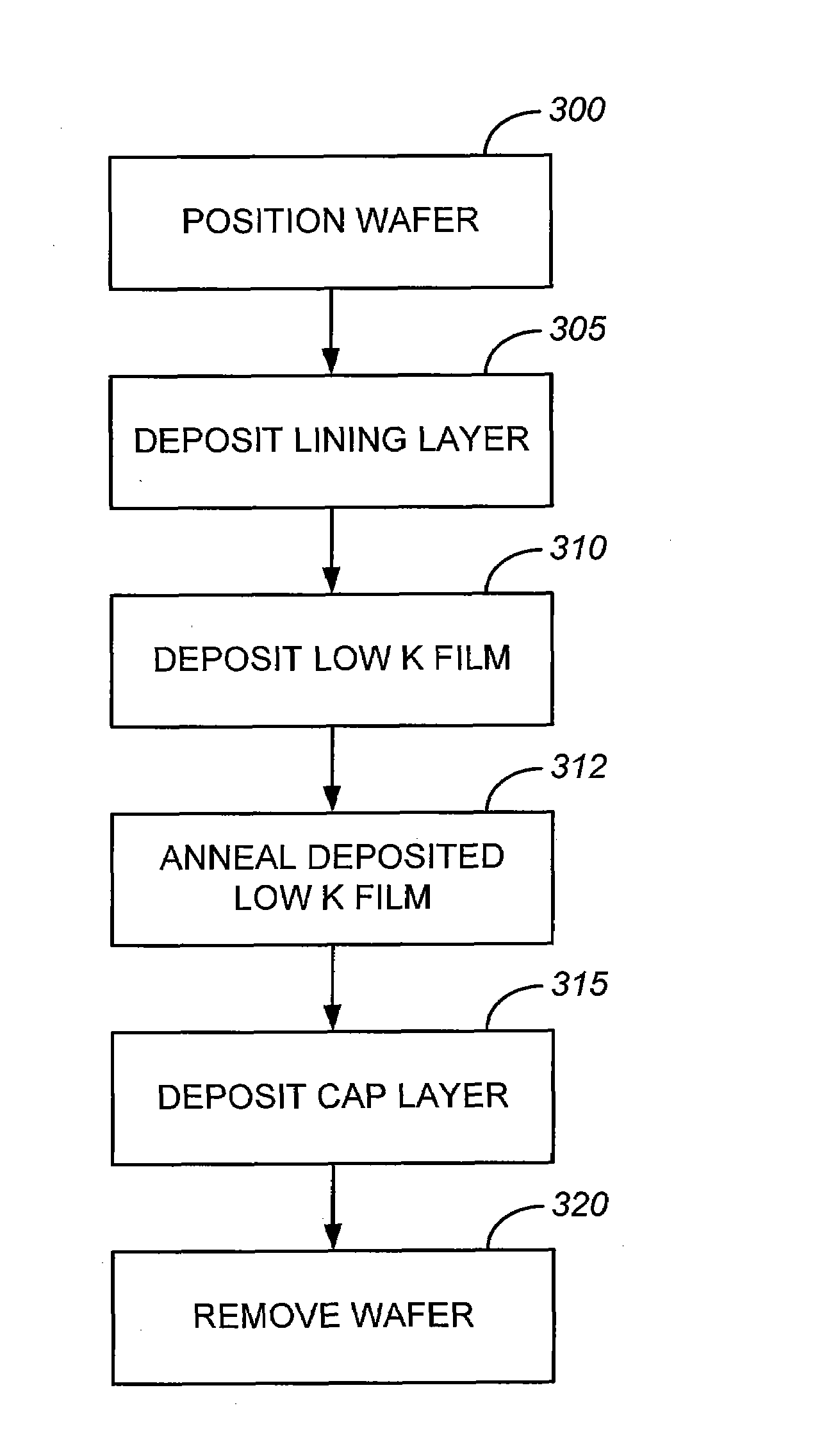
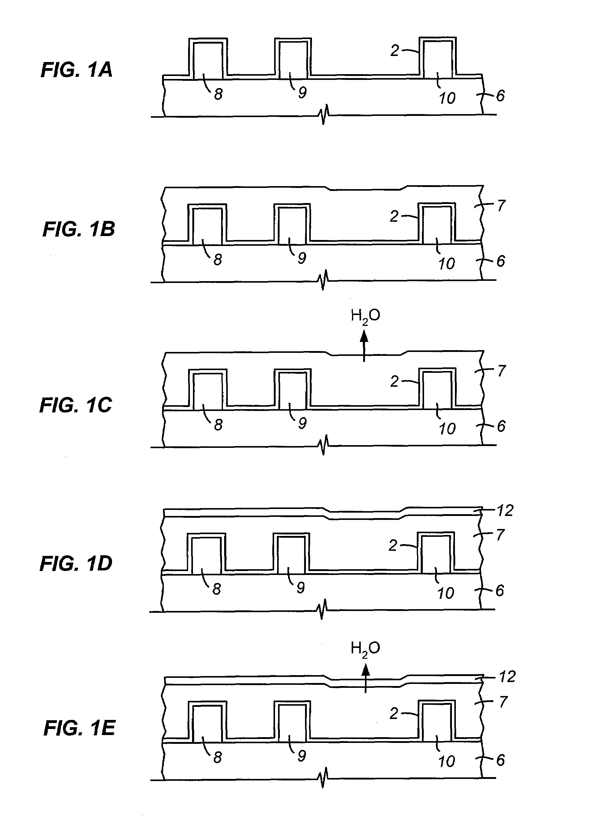
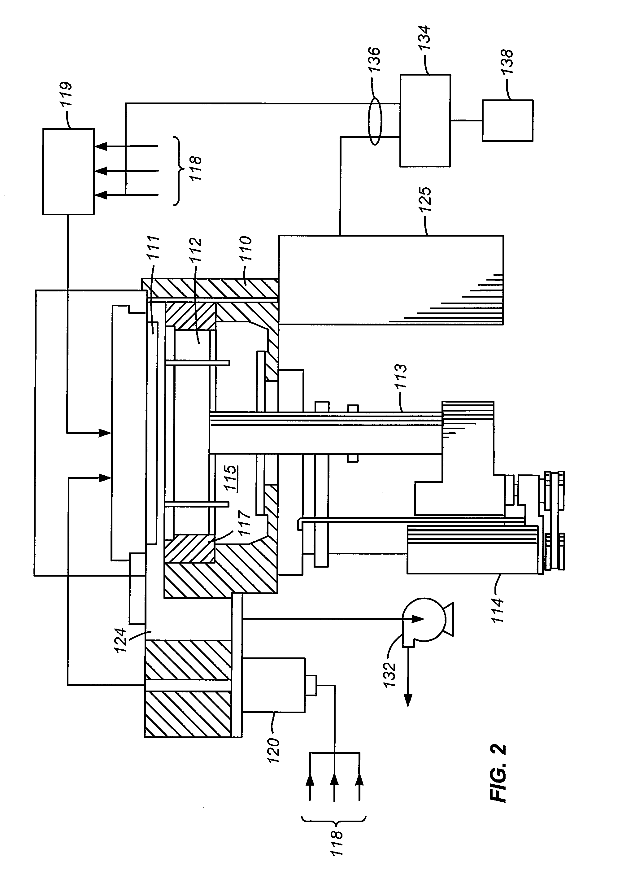
[0119]The following examples demonstrate deposition of a nano-porous silicon oxide based film having dispersed microscopic gas voids. This example is undertaken using a chemical vapor deposition chamber, and in particular, a CENTURA “DLK” system fabricated and sold by Applied Materials, Inc., Santa Clara, Calif.

Silicon Compound Having Silicon Containing and Thermally Labile Imparting Components (Hypothetical)

[0120]A nano-porous silicon oxide based film is deposited at a chamber pressure of 1.0 Torr and temperature of 30° C. from reactive gases which are vaporized and flown into the reactor as follows:

[0121]

methylsilyl-2-furyl ether, at 150 sccmnitrous oxide (N2O), at1000 sccm

[0122]Prior to entering the chamber, the nitrous oxide is dissociated in a microwave applicator that provides 2000 W of microwave energy. The substrate is positioned 600 mil from the gas distribution showerhead and the reactive gases are introduced for 2 minutes. The substrate is then heated over a time period o...


PUM

PropertyMeasurementUnit
temperatureaaaaaaaaaa
dielectric constantaaaaaaaaaa
feature sizesaaaaaaaaaa

Abstract

Low K dielectric films exhibiting low mechanical stress may be formed utilizing various techniques in accordance with the present invention. In one embodiment, carbon-containing silicon oxide films are formed by plasma-assisted chemical vapor deposition at low temperatures (300° C. or less). In accordance with another embodiment, as-deposited carbon containing silicon oxide films incorporate a porogen whose subsequent liberation reduces film stress.

Description

CROSS-REFERENCE TO RELATED APPLICATION[0001]This nonprovisional patent application claims priority to U.S. provisional patent application No. 60 / 604,316, filed Aug. 24, 2004, which is incorporated by reference herein for all purposes.BACKGROUND OF THE INVENTION[0002]One of the primary steps in the fabrication of modern semiconductor devices is the formation of metal and dielectric films on a substrate by chemical reaction of gases. Such deposition processes are referred to as chemical vapor deposition or CVD. Conventional thermal CVD processes supply reactive gases to the substrate surface where heat-induced chemical reactions take place to produce a desired film. The high temperatures at which some thermal CVD processes operate can damage device structures having layers previously formed on the substrate. A preferred method of depositing metal and dielectric films at relatively low temperatures is plasma-enhanced CVD (PECVD) techniques such as described in U.S. Pat. No. 5,362,526, ...

Claims


Application Information

Patent Timeline
Patent Type & Authority Patents(United States)
IPC IPC(8): H05H1/24
CPCC23C16/401C23C16/56H01L21/02126H01L21/02203H01L21/02304H01L21/76835H01L21/02362H01L21/31633H01L21/31695H01L21/76802H01L21/76811H01L21/02351H01L21/02274
Inventor YIM, KANG SUBHUANG, LIHUA LISCHMITT, FRANCIMARXIA, LI-QUN
Owner APPLIED MATERIALS INC
Why Eureka
Try Eureka