Signal processing device and image pickup apparatus using the same

Active Publication Date: 2008-09-30
CANON KK
View PDF26 Cites 86 Cited by
  • Summary
  • Abstract
  • Description
  • Claims
  • Application Information

AI Technical Summary

Benefits of technology

[0024]It is an object of the invention to provide a signal processing device capable of suppressing a voltage change of a power supply when output signals from a plural

Problems solved by technology

In some cases, this clock noise is superposed upon an output from the read common amplifier and the incorrect output is obtained.
Shading may also occur because of this clock noise.
However, the resistance of this wiring pattern cannot be

Method used


Image

  • Signal processing device and image pickup apparatus using the same
  • Signal processing device and image pickup apparatus using the same
  • Signal processing device and image pickup apparatus using the same

Examples


first embodiment

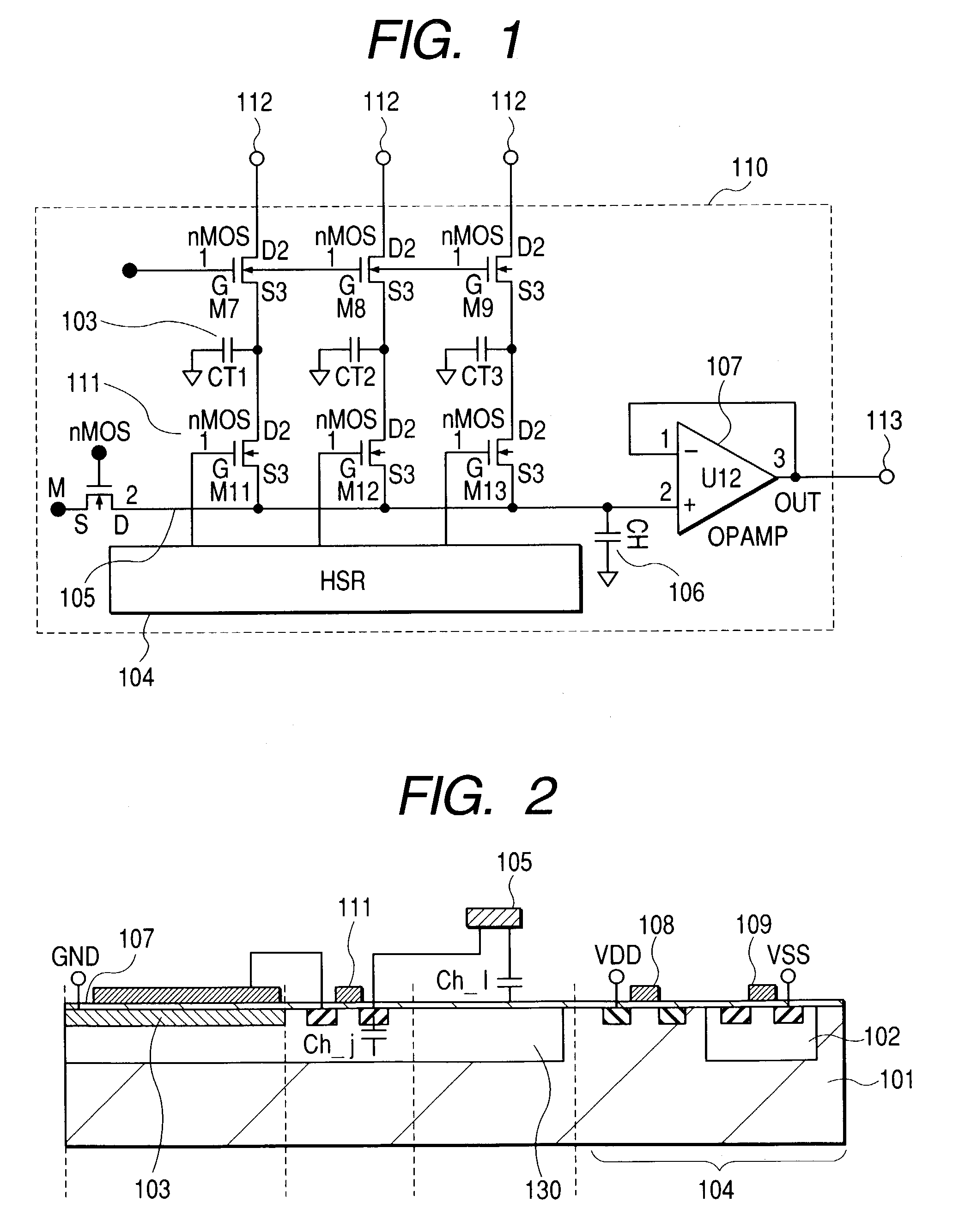
[0045]FIG. 1 is a circuit diagram of a signal processing device according to the first embodiment of the invention. In FIG. 1, reference numeral 112 represents a plurality of terminals connected to a plurality of signal wiring lines connected to signal sources. Reference numeral 110 represents a read circuit for converting parallel signals transferred via the terminals 112 into serial signals and outputting them, and reference numeral 113 represents a terminal for connection of an output signal output from a read common amplifier 107 to another suitable circuit for use.

[0046]The terminal 113 is connected to an A / D converter circuit (not shown).

[0047]Alternatively, the A / D converter circuit (not shown) may be provided in the read circuit 110 and connected via the terminal 113 to a processing circuit such as a memory or the like.

[0048]Reference numeral 103 represents a holding capacitor (CT) for holding an output signal supplied from a signal source (not shown) via a vertical output l...

second embodiment

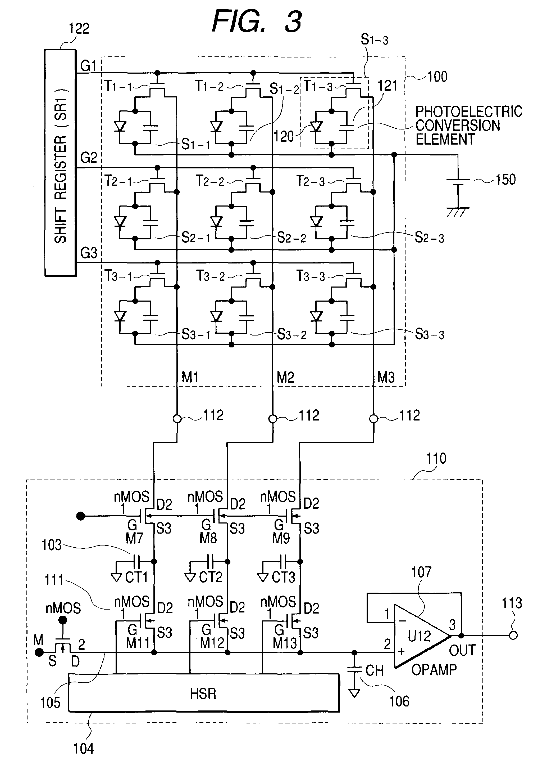
[0056]FIG. 3 is a circuit diagram of an image pickup device according to the second embodiment of the invention. In FIG. 3, reference numeral 100 represents a photoelectric conversion circuit, reference numeral 120 represents a light reception area for converting incident light into signal charges, reference numeral 121 represents an inter-electrode capacitor for accumulating the signal charges photoelectrically converted by the light reception area 120, and St-t (t=1 to 3) represents a pixel having the light reception area 120, the inter-electrode capacitor 121 and a switching element Tt-t. For example, a pixel S1-3 has a light reception area 120, an inter-electrode capacitor 121 and a switching element T1-3.

[0057]Each of the pixels S1-1 to S3-3 may have an amplifier transistor and / or a reset transistor, depending upon its use. FIG. 4 is a circuit diagram showing another structure of a pixel applicable to the image pickup apparatus. In FIG. 4, reference numeral 140 represents a uni...

third embodiment

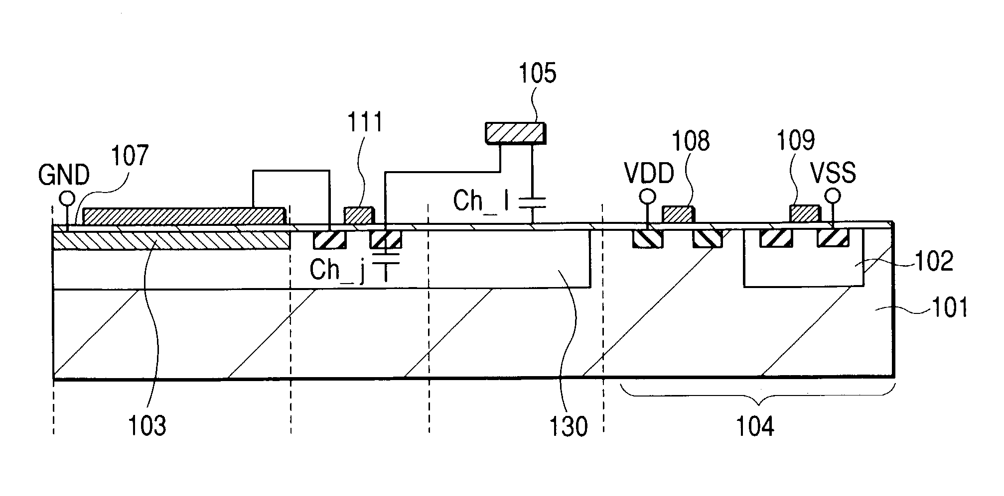
[0065]FIG. 5 is a schematic cross sectional view of a signal processing device according to the third embodiment of the invention.

[0066]The circuit diagram of this embodiment is similar to that shown in FIG. 1.

[0067]Elements represented by identical reference symbols and numerals have already been described and the description thereof is omitted.

[0068]Similar to the circuit shown in FIG. 1, the transfer switch 111 is required in order to read an output signal held in the holding capacitor 103 to the horizontal common signal line 105. This transfer switch 111 is turned on and off by the horizontal scanning circuit 104 disposed opposite to the holding capacitor 103 with the horizontal common signal line 105 being interposed therebetween. In this case, the control signal supplied from the horizontal scanning circuit 104 is transferred via a signal line disposed under the horizontal common signal line 105.

[0069]More specifically, in FIG. 5, reference numeral 212 represents a logic signa...


PUM


Abstract

A signal processing device is provided which is capable of suppressing a voltage change of a power supply when output signals from a plurality of signal sources are read, and capable of outputting a stable signal at a high sensitivity, and an image pickup apparatus using such a signal processing device is also provided. The signal processing device has: a plurality of terminals connectable to a plurality of signal sources; and a read circuit for converting signals input from the terminals into serial signals and outputting the serial signals, wherein: the read circuit comprises a holding capacitor connected to each of the terminals, a transfer switch for transferring a signal held in the holding capacitor to a common signal line, and a shift register for driving the transfer switch; and a semiconductor layer under the common signal line has a conductivity type opposite to a first conductivity type of a semiconductor substrate.

Description

BACKGROUND OF THE INVENTION[0001]1. Field of the Invention[0002]The present invention relates to a signal processing device having a circuit portion of temporarily storing a plurality of output signals and then reading the stored signals and to an image pickup apparatus using such a device.[0003]2. Description of the Related Art[0004]FIG. 13 is a circuit diagram of an image pickup apparatus utilizing a signal processing device having a conventional structure.[0005]In a conventional line sensor or area sensor, output signals from pixels 1001 are once held in holding capacitors 1003 via vertical output lines 1002, thereafter, the output signals held in the holding capacitors are sequentially read to a horizontal common signal line 1005 by a horizontal scanning circuit 1004, and output to a common read amplifier 1007.[0006]An output from the holding capacitor 1003 to the horizontal common signal line 1005 is determined by a capacitor division of a capacitance CT of the holding capacito...

Claims


Application Information

Patent Timeline
IPC IPC(8): H01L31/062H01L31/113H01L21/768H01L21/822H01L23/522H01L27/04H01L27/146H01L31/10H04N5/335H04N5/361H04N5/369H04N5/374H04N5/378
CPCH04N5/3577H04N5/378H04N5/359H04N25/62H04N25/617H04N25/75
Inventor KOIZUMI, TORUSAKURAI, KATSUHITOHIYAMA, HIROKIFUJIMURA, MASARU
Owner CANON KK
Why Eureka
Try Eureka