

Materials for forming capacitor layer and printed wiring board having embedded capacitor circuit obtained by using the same
a technology of printed wiring board and capacitor, which is applied in the direction of fixed capacitor details, printed circuit non-printed electric components association, fixed capacitors, etc., can solve the problems of dielectric layer and nickel-phosphorus alloy layer delamination, limit in improvement of surface area (a), and sometimes occur nickel-phosphorus alloy layers. , to achieve excellent adhesion, the effect of capacitor circuit formation
- Summary
- Abstract
- Description
- Claims
- Application Information
AI Technical Summary
Benefits of technology
Problems solved by technology
Method used
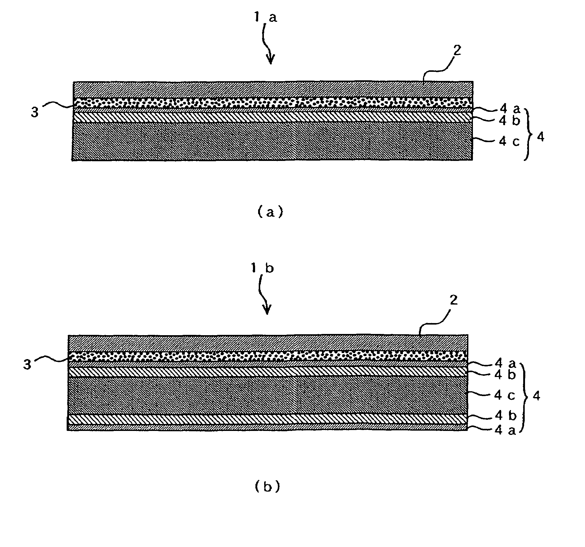
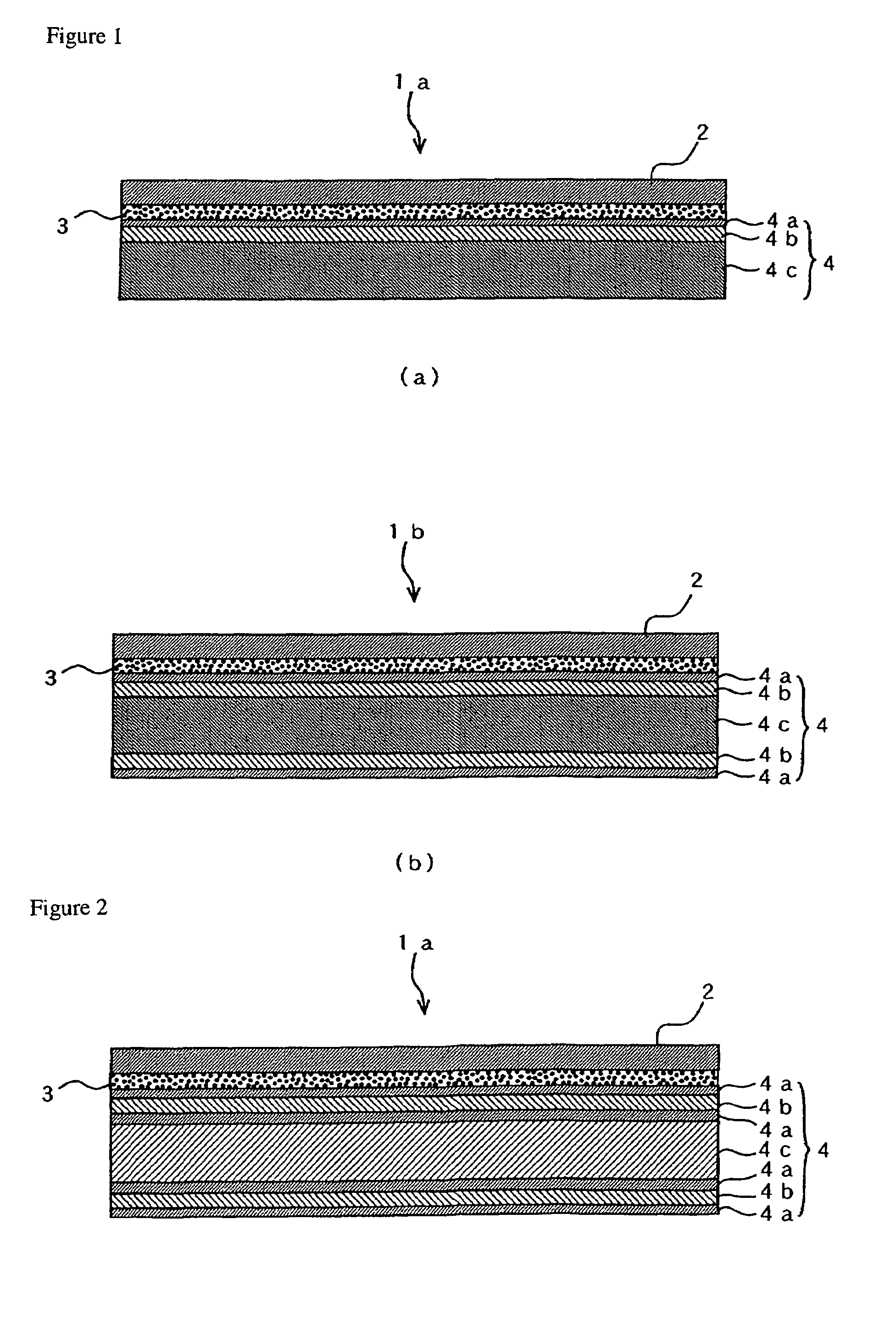
Image

Examples
embodiment 1
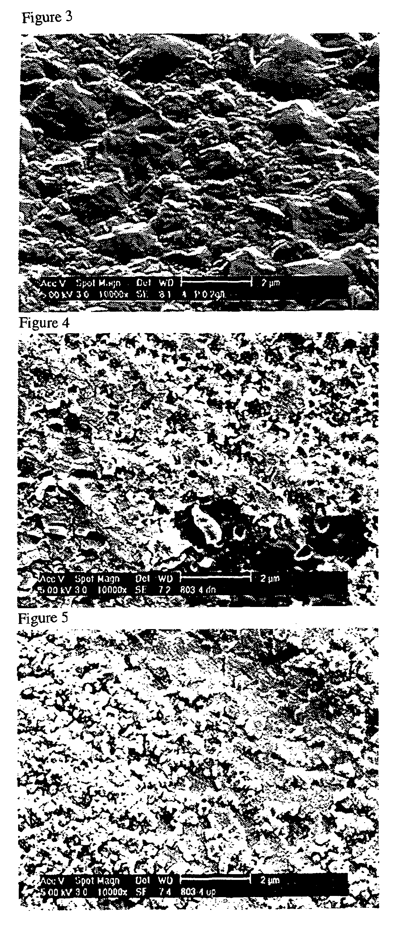
[0044]Production of surface treated copper foil used for the formation of a second conductive layer:
[0045]An about 2 μm thick pure nickel layer and an about 1.0 μm thick nickel-phosphorus alloy layer were formed on both surfaces of 35 μm thick electrodeposited copper foil by the electrolytic plating method. The phosphorus content in the nickel-phosphorus alloy layer at this time was 0.3 wt %. In the formation of the pure nickel layer, a nickel sulfate bath with the following conditions is used. A nickel sulfate concentration of 240 g / l, a nickel chloride concentration of 45 g / l, an H3BO3, concentration of 30 g / l, a solution temperature of 50° C., a pH of 4.5, and a current density of 5 A / dm2. Then a 2 μm thick pure nickel layer was electrodeposited uniformly and smoothly on both surfaces of the electro deposited copper foil. For the nickel-phosphorus alloy layer, electrolysis was performed by using a phosphoric-acid-based solution with the following conditions. A nickel sulfate conc...
PUM
| Property | Measurement | Unit |
|---|---|---|
| thicknesses | aaaaa | aaaaa |
| thicknesses | aaaaa | aaaaa |
| thickness | aaaaa | aaaaa |
Abstract
Description
Claims
Application Information