

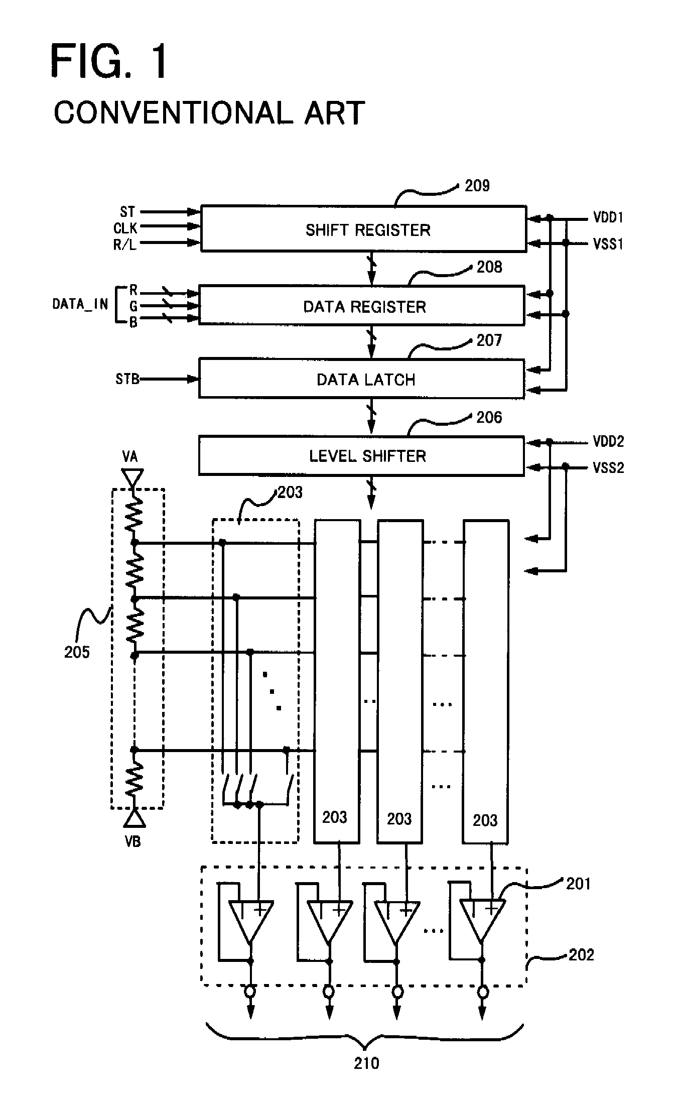
Differential amplifier, digital-to-analog converter and display device
a technology of digital to analog converter and display device, which is applied in the direction of differential amplifier, amplifier with semiconductor device/discharge tube, amplifier details, etc., can solve the problems of increasing die cost, limitation of offset suppressing effect, and document 1, 2 and 3
- Summary
- Abstract
- Description
- Claims
- Application Information
AI Technical Summary
Benefits of technology
Problems solved by technology
Method used
Image

Examples
first example
Third Modification of First Example
[0303]A further modification of this example will now be described. In this modification, an internally divided voltage can be generated and output with high precision at an internal dividing ratio other than (1:2). In the third modification, in which use is made of a circuit configuration identical with that of FIG. 9 (the first example), the transistor sizes and the current values of the current sources are set as indicated below. The ratio of the gate widths Wa1, Wb1, Wa2 and Wb2 of transistors Ma1, Mb1, Ma2 and Mb2, respectively, of the two differential pairs and the current ratio of the current sources I1 and I2 are set as indicated below. Switch control is similar to that shown in FIG. 10.
Wa1:Wb1:Wa2:Wb2=a2:a2:b2:b2 (37)
I1:I2=1:1 (38)
[0304]The following Equations (39) to (44) hold in period T01:
[0305]Ia1=Ib2(39)Ib1=Ia2(40)Ia1=12×a2βn{(Vin1-VS1)-Vthna1}2(41)Ib1=12×a2βn{(Vout-VS1)-Vthnb1}2(42)Ia2=12×b2βn{(Vin2-...
second example
[0325]A second example of the present invention will be described with reference to the accompanying drawings in regard to implementation of a multi-level-output in a case where three input voltages are applied.
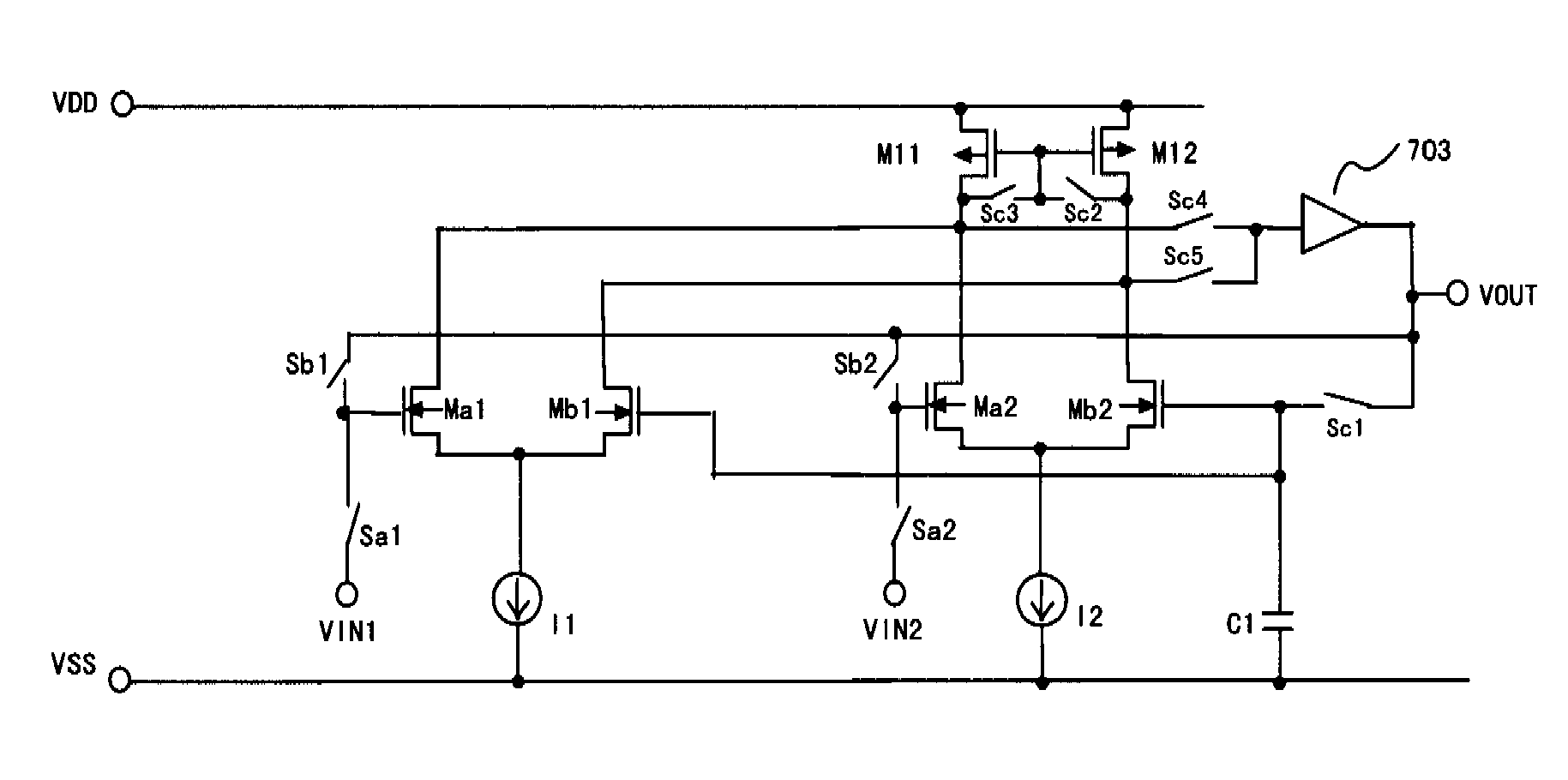
[0326]The circuit configuration of the second example of the present invention will now be described. FIG. 20 is a diagram illustrating the configuration of a differential amplifier according to the second example. The differential amplifier according to this example comprises: first differential pair (Ma1, Mb1) driven by current source 11; second differential pair (Ma2, Mb2) driven by current source 12; third differential pair (Ma3, Mb3) driven by current source 13; current mirror load circuit (M11, M12) to which the output pairs of the differential pairs are connected in common; and output-stage amplifying circuit 703.
[0327]Input terminal VIN1 is connected to the gate of one transistor Ma1 of the differential inputs of the first differential pair via switch Sa1, and the out...
third example
[0336]The circuit configuration of a third example of the present invention will now be described. FIG. 23 is a diagram showing the configuration of a differential amplifier according to the third example. For example, the differential amplifier shown in FIG. 23 employs the differential amplifier (FIG. 9) shown in the first example of the present invention. In the third example, the amplifier is further provided with an output switch SWout.
[0337]Switch control of the differential amplifier shown in FIG. 9 is carried out at the timing shown in FIG. 10. The output switch SWout in the third example is set in an OFF state in the offset detection period T01 and in an ON state in the offset-compensated output period T02.
[0338]By using the third example of FIG. 23, the amplifier stage output PB of the differential amplifier is cut off from an external (not shown) such as a data line in the offset detection period T01. As a result, the load is essentially the capacitor C1 for detecting offs...
PUM
 Abstract
Description
Claims
Application Information