High-density plasma hydrogenation

a plasma hydrogenation and high-density technology, applied in the direction of crystal growth process, coating, chemistry apparatus and processes, etc., can solve the problems of high inefficiency of forming gas annealing process for high-throughput commercial applications, preventing the generation of particularly reactive hydrogen species by coupled electrodes, and high inefficiency of fga process for low-temperature devices. achieve the effect of enhancing the concentration and state of active hydrogen species, enhancing the concentration and state of active hydrogen

Inactive Publication Date: 2008-11-04
SHARP KK
View PDF9 Cites 16 Cited by
  • Summary
  • Abstract
  • Description
  • Claims
  • Application Information

AI Technical Summary

Benefits of technology

[0012]The present invention describes the hydrogenation of polysilicon films and Si / SiO2 interfaces, at a significantly lower thermal budget, using a high-density hydrogen plasma treatment. As compared to conventional processes, the efficiency of the present invention hydrogenation process is as a result of enhancing the concentration and state of active hydrogen species. The high plasma density and energy of the high-density plasma process makes it possible to generate active hydrogen species, to achieve the efficient hydrogenation of polysilicon layers and Si / SiO2 interfaces at a lower temperature and thermal budget than conventional FGA and plasma processes. The present invention hydrogenation process can be carried out at temperatures of less than 400° C., making it suitable for the low temperature integration of devices on glass or other temperature-sensitive substrates.

Problems solved by technology

The FGA process is highly inefficient for the low temperature devices due to very low rate diffusion kinetics.
Due to the high thermal budget, the forming gas annealing process is not efficient for high throughput commercial applications.
However, the limitations associated with coupled electrodes prevent the generation of an especially reactive hydrogen species.

Method used


Image

  • High-density plasma hydrogenation
  • High-density plasma hydrogenation
  • High-density plasma hydrogenation

Examples


Embodiment Construction

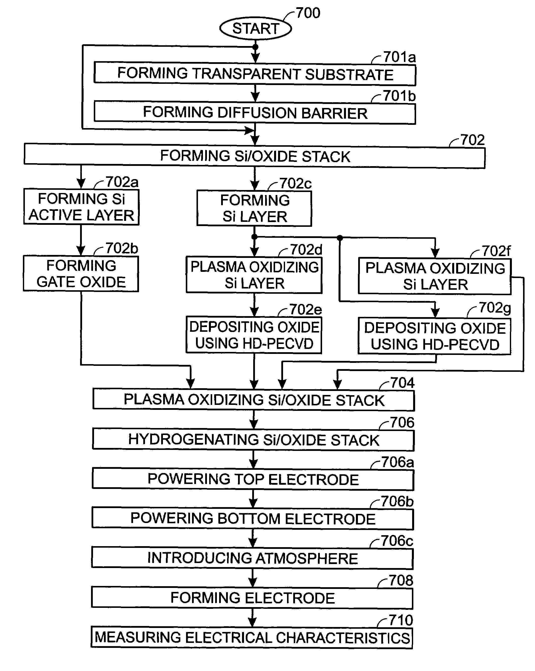
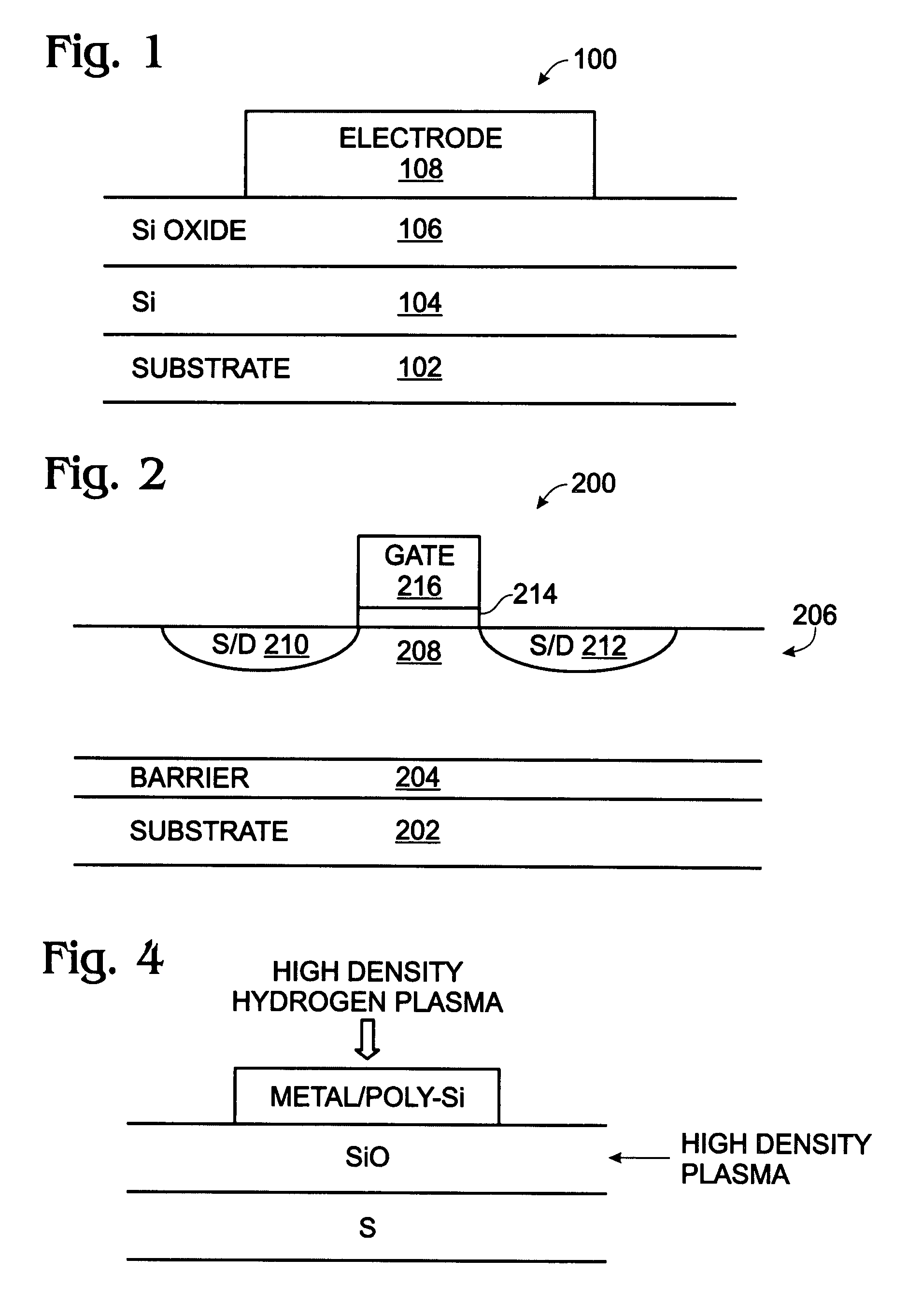
[0023]FIG. 1 is a partial cross-sectional view of a capacitor device with a hydrogenated oxide interface. The device 100 comprises a transparent substrate 102, sensitive to process temperatures of greater than 600 degrees C. For example, the transparent substrate 102 can be glass, quartz, or plastic. A silicon (Si) film 104 overlies the transparent substrate 102. Note, is some aspects a diffusion barrier (not shown) of a material such as SiO2 or SiOxNy, may separate the Si film 104 and transparent substrate 102. An oxide layer 106 overlies the Si film 104, and a conductive electrode 108 overlies the oxide layer 106. The oxide layer 106 has an interface trap concentration (Dit) of less than 5×10¹⁰ eV−1cm−2, a leakage current density of less than 1×10⁻⁸ A / cm2 (at 2 MV / cm), and a breakdown field of greater than 8 MV / cm.

[0024]FIG. 2 is a partial cross-sectional view of a liquid crystal display (LCD) thin-film transistor (TFT). The TFT 200 comprises a temperature sensitive transparent su...


PUM

PropertyMeasurementUnit
temperatureaaaaaaaaaa
frequencyaaaaaaaaaa
pressureaaaaaaaaaa

Abstract

A high-density plasma hydrogenation method is provided. Generally, the method comprises: forming a silicon (Si) / oxide stack layer; plasma oxidizing the Si / oxide stack at a temperature of less than 400° C., using a high density plasma source, such as an inductively coupled plasma (ICP) source; introducing an atmosphere including H2 at a system pressure up to 500 milliTorr; hydrogenating the stack at a temperature of less than 400 degrees C., using the high density plasma source; and forming an electrode overlying the oxide. The electrode may be formed either before or after the hydrogenation. The Si / oxide stack may be formed in a number of ways. In one aspect, a Si layer is formed, and the silicon layer is plasma oxidized at a temperature of less than 400 degrees C., using an ICP source. The oxide formation, additional oxidation, and hydrogenation steps can be conducted in-situ in a common chamber.

Description

RELATED APPLICATIONS[0001]This application is a continuation-in-part of a patent application entitled, PLASMA PROCESS FOR SILICON THIN FILMS, invented by Pooran Joshi, et al., Ser. No. 10 / 871,939, filed Jun. 17, 2004 now U.S. Pat. No. 7,186,663.[0002]This application is a continuation-in-part of a patent application entitled, METHODS FOR FABRICATING OXIDE THIN FILMS, invented by Pooran Joshi et al., Ser. No. 10 / 801,374, filed Mar. 15, 2004 now U.S. Pat. No. 7,087,537. These applications, and their parent applications, are incorporated herein by reference.BACKGROUND OF THE INVENTION[0003]1. Field of the Invention[0004]This invention generally relates to the fabrication of integrated circuit (IC) devices, and more particularly, to a hydrogenated oxide interface on silicon and a method for forming the same using high-density hydrogen plasma.[0005]2. Description of the Related Art[0006]The quality of polysilicon thin films and the interface between silicon and silicon dioxide (Si / SiO2) ...

Claims


Application Information

Patent Timeline
Patent Type & Authority Patents(United States)
IPC IPC(8): H01L21/332B05D5/12H01L29/872C23C16/24C23C16/455C23C16/509C30B1/00H01L21/00H01L21/04H01L21/20H01L21/205H01L21/31H01L21/316H01L21/36H01L21/42H01L21/469H01L29/47H01L29/786
CPCH01L29/4908H01L21/02532C23C16/24C23C16/45523C23C16/509H01L21/31612H01L21/28194H01L21/28211H01L21/3003H01L29/513H01L21/02381H01L21/0242H01L21/02422H01L21/0245H01L29/78609H01L21/02164H01L21/02274H01L21/02323H01L21/022H01L21/0234
Inventor JOSHI, POORAN CHANDRAVOUTSAS, APOSTOLOS T.HARTZELL, JOHN W.
Owner SHARP KK
Why Eureka
Try Eureka