Methods and system for improving integrated circuit layout

a technology of integrated circuits and layouts, applied in the field of integrated circuit manufacturing, can solve the problems of systematic yield failure, waste of chip area, and difficult capture of feature-dependent interactions with precise design rules, and achieve the effect of reducing guard bands and improving chip yield

Active Publication Date: 2008-11-04
IYM TECH
View PDF33 Cites 33 Cited by
  • Summary
  • Abstract
  • Description
  • Claims
  • Application Information

AI Technical Summary

Benefits of technology

[0009]The present invention provides a local process modification value to the basic design rule constraint. Local process modification represents an additional safeguard distance beyond the design rule constraint distance. The local process modification value can be calculated from simulated process responses in the region of interest, with a predetermined, often empirical, equation, or from look-up data tables. The original design rule distance plus local process modification effectively creates a new constraint for every unique local situation. With this additional local safeguard, we can reduce the guard band in design rule formulation and improve chip yield by eliminating processing hotspots arising from low

Problems solved by technology

Failure to capture the absolute worst case in all chips would lead to systematic yield failure.
For this reason, the feature dependent interactions are difficult to capture with precise design rules.
The drawback of this approach is at least two fold: firstly, it clearly wastes chip ar

Method used


Image

  • Methods and system for improving integrated circuit layout
  • Methods and system for improving integrated circuit layout
  • Methods and system for improving integrated circuit layout

Examples


Embodiment Construction

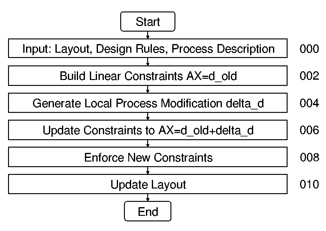
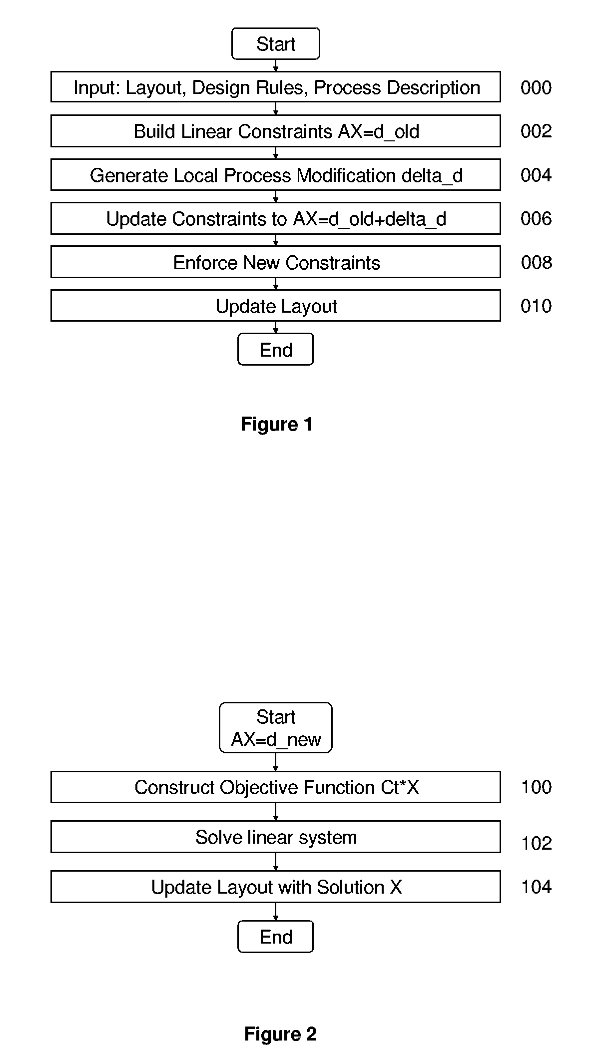
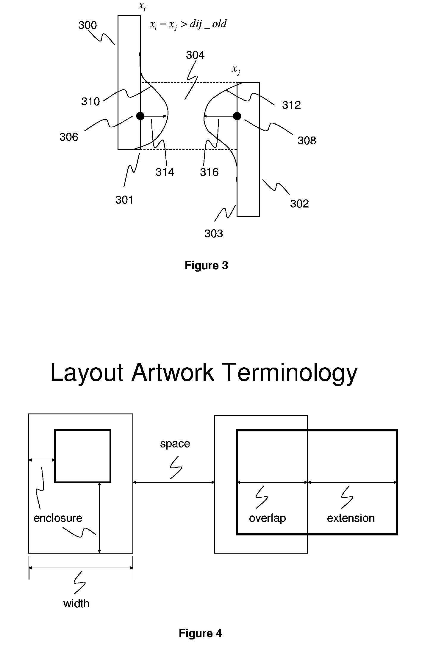
[0022]Some preferred embodiments of the present invention will be described in detail with reference to the related drawings of FIGS. 1-8. Additional embodiments, features and / or advantages of the invention will become apparent from the ensuing description or may be learned by the practice of the invention.

[0023]The methods and apparatus described here are with respect to integrated circuit manufacturing; however, the techniques described here can be applied to manufacturing or design of any device that require pattern transfer from a polygon database drawing to physical materials using lithographic and / or etch methods. Examples of these include integrated optical devices, microelectromechanical systems (MEMS), gene chips, micromachines, disk drive heads, etc.

[0024]The following description includes the best mode presently contemplated for carrying out the invention. This description is not to be taken in a limiting sense, but is made merely for describing the general principles of ...


PUM


Abstract

In accordance with the present method and system for improving integrated circuit layout, a local process modification is calculated from simulated process response variables at a set of control points. Said modification values are incorporated into the layout constraints imposed by design rules and design intent to account for manufacturing friendliness. Solving the updated constraint equation with user specified objective function produces a new layout with increased manufacturability. The new layout may further contain data tags that enable optimal process correction to be performed on selected locations, leading to reduction in data size and mask complexity. Also in accordance with this invention, physical design tools are enhanced to read and process anisotropic design rules.

Description

[0001]This application claims the benefits of U.S. Provisional Patent Application Ser. No. 60 / 564,082 filed on Apr. 21, 2004, and U.S. Provisional Patent Application Ser. No. 60 / 603,758 filed on Aug. 23, 2004.FIELD OF THE INVENTION[0002]The present invention relates generally to integrated-circuit manufacturing and more particularly to methods and system for generating and optimizing its layout artwork.PRIOR ART[0003]In modern processing technology, the manufacturing yield of an integrated circuit depends heavily on its layout construction. For a given manufacturing process, a corresponding set of design rules are applied during chip layout to avoid geometry patterns that can cause chip failure. These design rules guarantee the yield by limiting layout geometry parameters such as minimum spacing, minimal line width, etc.[0004]Existing layout construction systems apply design rules over a wide chip area, and to entire classes of circuits. For this reason, the design rule must cover t...

Claims


Application Information

Patent Timeline
IPC IPC(8): G06F17/50
CPCG06F17/5068G06F30/39G03F1/70G06F30/398G06F30/392G06F30/394G06F30/323H01L27/0207
Inventor QIAN, QI-DE
Owner IYM TECH
Why Eureka
Try Eureka