Semiconductor package substrate with embedded chip and fabrication method thereof

a technology of semiconductor packaging and embedded chips, which is applied in the direction of semiconductor/solid-state device details, electrical equipment, semiconductor devices, etc., can solve the problems of increasing fabrication costs, sn—pb materials have relatively high costs, and the above-mentioned package fabrication process uses a large amount, so as to simplify the semiconductor fabrication process and meet the requirements of clients. , the effect of good heat dissipation and electromagnetic shielding

Active Publication Date: 2008-11-11
PHOENIX PRECISION TECH CORP
View PDF9 Cites 61 Cited by
  • Summary
  • Abstract
  • Description
  • Claims
  • Application Information

AI Technical Summary

Benefits of technology

[0009]In light of the above drawbacks in the prior art, an objective of the present invention is to provide a semiconductor package substrate with embedded chip and a fabrication method thereof, which can integrate fabrication processes of a chip support plate and semiconductor packaging processes, so as to provide greater flexibility for clients' requirements and simplify semiconductor fabrication processes and an interface integration problem.
[0010]Another objective of the present invention is to provide a semiconductor package substrate with embedded chip and a fabrication method thereof, so as to effectively dissipate heat produced by operation of a semiconductor-chip.
[0011]Still another objective of the present invention is to provide a semiconductor package substrate with embedded chip and a fabrication method thereof, which can prevent problems such as flashes during an encapsulation process, failure in effective filling and so on in packaging processes for a chip and a receiving base material in the prior art, so as to effectively improve production quality and product reliability.
[0012]A further objective of the present invention is to provide a semiconductor package substrate with embedded chip and a fabrication method thereof, by which an insulating layer is used to fix a semiconductor chip and as a material for a circuit patterning process, so as to save materials and reduce fabrication costs.
[0015]Therefore, the present invention can combine fabrication processes of a chip carrier and semiconductor packaging processes by integrating the metallic layer, the semiconductor chip and a circuit structure, so as to provide greater flexibility for clients' requirements and simplify semiconductor fabrication processes and an interface integration problem. Further in the present invention, the semiconductor chip is mounted on the metallic board, for providing good heat dissipating and electromagnetic shielding effects. Moreover, the present invention does not use a large amount of Sn—Pb materials for electrical connection, thereby saving material costs and preventing an environmental problem. And in the present invention, copper circuits are directly formed on the semiconductor chip, for providing electrical connection and extension, so as to shorten an electrical connection path and effectively improve overall electrical performances. Furthermore, in the present invention, a first insulating layer that has not been completely cured and the semiconductor chip are firstly mounted on the metallic board, and then a support plate having a predetermined through cavity for receiving the semiconductor chip is mounted on the first insulating layer and a second insulating layer is pressed on the support plate by heating, so as to allow insulating materials of the first and second insulating layers to fill a gap between the semiconductor chip and the support plate, and effectively fix the semiconductor chip in the through cavity of the support plate. The second insulating layer also serves as a material required for a subsequent circuit fabrication process, such that material costs are saved, and a reliability problem due to chip contamination by flashes during an encapsulation process in conventional semiconductor packaging processes can be prevented, as well as a process stability problem such as a popcorn effect in a thermal cycle of a subsequent circuit stacking process caused by difficulty in effectively filling the gap between the semiconductor chip and the support plate by an encapsulating resin can be prevented.

Problems solved by technology

However, the foregoing package fabrication processes uses a large amount of Sn—Pb materials for electrical connection.
The Sn—Pb materials have relatively high costs, making fabrication costs increased and causing an environmental problem due to the materials containing Pb.
Moreover, an electrical connection path of conductive circuits is relatively lengthy in the above package, thereby not able to improve overall electrical performance.
Although the BBUL technique can solve the problem of chip electrical connection, in BBUL packaging processes due to mismatch in coefficient of thermal expansion (CTE) between a semiconductor material (such as a chip) and a receiving base material, breakage or cracks of layout circuits may be caused.
However, the underfilling process not only increase fabrication steps but also easily leads to a problem such as flashes due to difficulty in control quality stability in fabrication; the flashes would contaminate the chip and thus adversely affect reliability of the fabrication processes.
Moreover, the encapsulating resin is different in material from a subsequent insulating layer required for circuit stacking, such that the underfilling process not only increase the fabrication steps but also easily causes a delamination problem.
In addition, during resin underfilling, due to the size of the gap between the chip and the base material, the encapsulating resin is not easy to effectively fill the small gap and thus causes voids in the gap, which would lead to a popcorn effect during a thermal cycle of a subsequent circuit stacking process and a subsequent reliability test.
This makes the quality stability of the BBUL package unsatisfactory and difficult to control, thereby not able to be widely accepted.
If the heat produced from the requirements of semiconductor packages, heat produced by operation of semiconductor chips cannot be timely and effectively dissipated, the performances and lifetime of the semiconductor chips would be severely affected.
Additionally, general semiconductor packages do not have effective shielding effects, which may be easily subject to external electromagnetic and noise interference and thus operation thereof would be adversely affected.

Method used


Image

  • Semiconductor package substrate with embedded chip and fabrication method thereof
  • Semiconductor package substrate with embedded chip and fabrication method thereof
  • Semiconductor package substrate with embedded chip and fabrication method thereof

Examples


Embodiment Construction

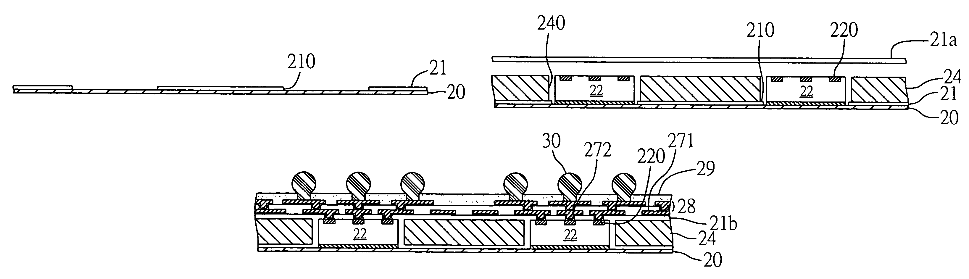
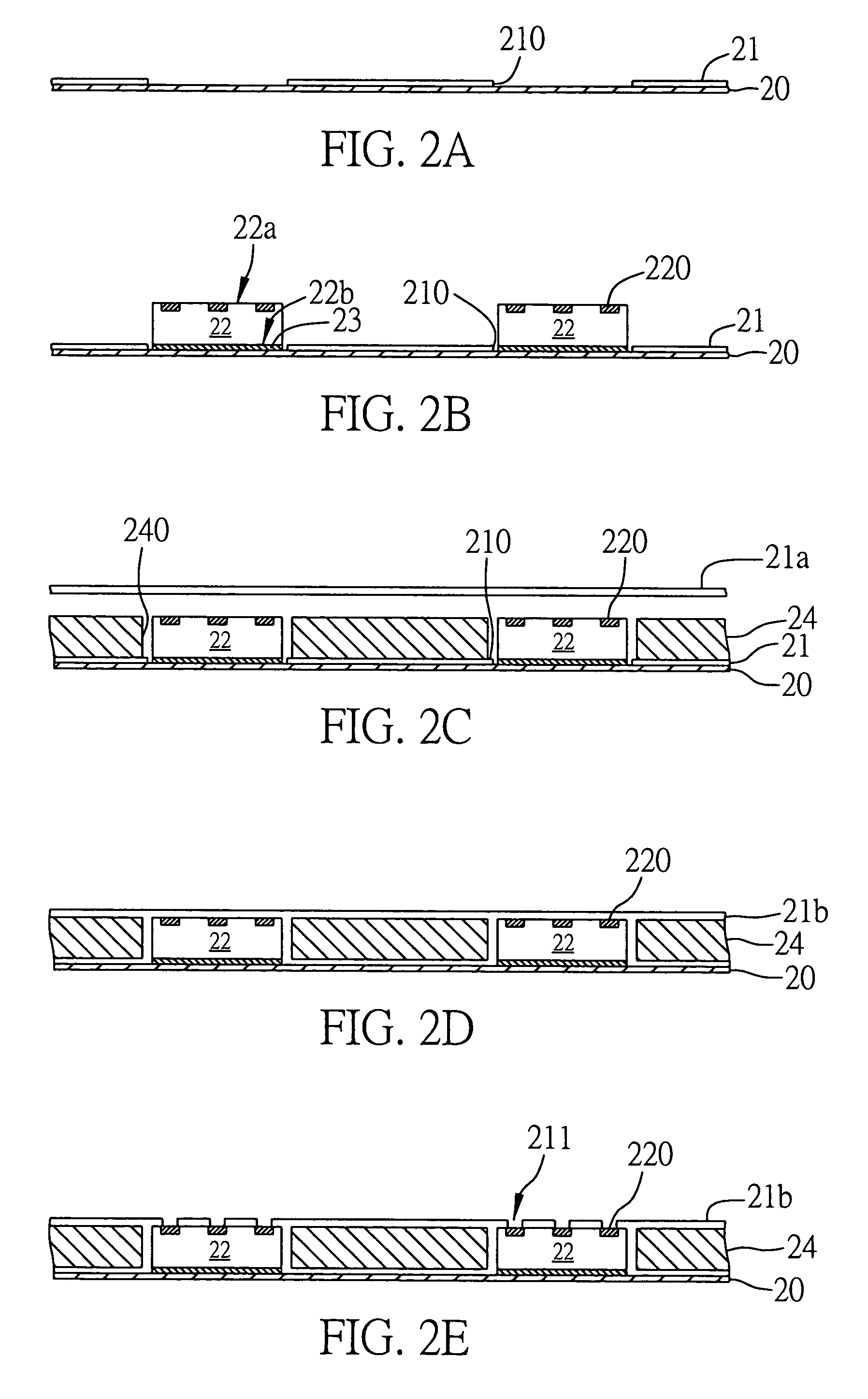
[0019]FIGS. 2A to 2J are cross-sectional schematic diagrams showing steps of a fabrication method of a semiconductor package substrate with embedded chip according to the present invention.

[0020]Referring to FIG. 2A, firstly a metallic board 20 is provided, and a first insulating layer 21 is applied on a surface of the metallic board 20, wherein the first insulating layer 21 applied on the metallic board has not been completely cured by baking and is formed with at least one opening 210 for exposing a portion of the metallic board 20. The metallic board 20 can be made of for example a copper foil. The first insulating layer 21 can be made of a material such as polyimide (PI), polytetrafluoroethylene (PTFE), ABF, bismaleimide triazine (BT), FR5 resin, or a mixture of organic resin and fillers, and so on.

[0021]Referring to FIG. 2B, a non-active surface 22b of at least one semiconductor chip 22 is mounted by a thermally conductive adhesive layer 23 on the portion of the metallic board ...


PUM


Abstract

A semiconductor package substrate with embedded chip and a fabrication method thereof are provided. A first insulating layer is applied on a metallic board, and formed with at least one opening for exposing a portion of the metallic board. At least one semiconductor chip is mounted on the exposed portion of the metallic board. A support plate is mounted on the first insulating layer, and formed with a through cavity at a position corresponding to the opening of the first insulating layer, for receiving the chip in the through cavity. A second insulating layer is applied on the chip and the support plate. Insulating materials of the insulating layers fill a gap between the chip and the support plate. A circuit layer is formed on the second insulating layer, wherein the circuit layer is electrically connected to the chip by conductive structures formed in the second insulating layer.

Description

FIELD OF THE INVENTION[0001]The present invention relates to semiconductor package substrates with embedded chips and fabrication methods thereof, and more particularly, to a semiconductor package substrate integrated with a heat sink, a semiconductor chip and a circuit structure, and a fabrication method of the semiconductor package substrate.BACKGROUND OF THE INVENTION[0002]Flip-chip semiconductor packaging technology has been introduced in early 1960s by the IBM company, which is characterized in using solder bumps for electrically connecting a semiconductor chip to a substrate instead of using general gold wires as compared with wire-bonding technology. The flip-chip technology yields significant advantages, for example increasing packaging density to reduce the size of package element, and improving electrical performance as not requiring relatively lengthy metallic wires. Accordingly, there has been proposed control-collapse chip connection (C4) technology to use high temperat...

Claims


Application Information

Patent Timeline
Patent Type & Authority Patents(United States)
IPC IPC(8): H01L21/50H01L21/44H01L23/02H01L23/12H01L23/24H01L21/48
CPCH01L24/24H01L23/5389H01L24/19H01L23/49816H01L2224/0401H01L2224/04105H01L2224/16225H01L2224/20H01L2224/24227H01L2224/73204H01L2224/92224H01L2224/92244H01L2924/01029H01L2924/01038H01L2924/01075H01L2924/01079H01L2924/01082H01L2924/14H01L2924/15153H01L2924/1517H01L2924/15174H01L2924/15311H01L2924/3025H01L2224/73267H01L2224/32245H01L2224/12105H01L2924/10253H01L2224/32225H01L2924/01033H01L2924/00H01L2924/351H01L2924/15787
Inventor HSU, SHIH-PING
Owner PHOENIX PRECISION TECH CORP
Why Eureka
Try Eureka