Field emission organic light emitting diode

a field emission and organic light technology, applied in the direction of discharge tube luminescnet screen, discharge tube/lamp details, cathode ray tube/electron beam tube, etc., can solve the problem of not meeting the requirement for high efficiency flat panel display, and achieve the effect of high luminescent efficiency

Inactive Publication Date: 2008-11-25
ITC LIMITED
View PDF8 Cites 13 Cited by
  • Summary
  • Abstract
  • Description
  • Claims
  • Application Information

AI Technical Summary

Benefits of technology

[0011]On the other hand, the inventor made a first-ever discovery of the organic electroluminescence principle. That is, the FEOLED luminescent mechanism is different from that of the traditional FED. In traditional FED, the inorganic phosphor illuminates as a result of electron beam bombardment. Whereas in FEOLED, the replacement of the inorganic phosphor by the organic EL light emitting layer results in a luminescent mechanism similar to that of the recombination mechanism found in OLED, only with higher luminescent efficiency.
[0012]This invention effectively integrates the luminescent characteristics of FED and OLED, yielding an FEOLED that is more efficient than the traditional OLED.

Problems solved by technology

Thus, it does not yet meet the requirement for high efficiency flat panel display.

Method used


Image

  • Field emission organic light emitting diode
  • Field emission organic light emitting diode
  • Field emission organic light emitting diode

Examples


fourth embodiment

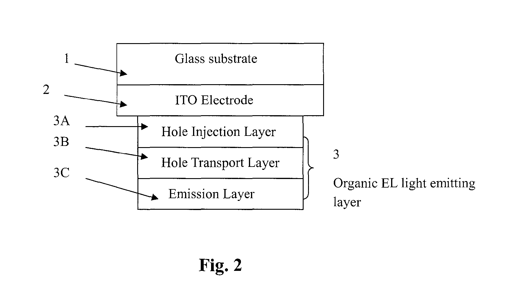
[0034]FIG. 9 shows the FEOLED device of the present invention. The multi-layer structure of the organic EL light emitting layer 3 has the same structure as that of FIG. 2 except for the metal back 10. The metal back 10 is attached to the secondary electron material coating on the emission layer 3C for adjusting EL intensity. The light color of the organic EL light emitting layer 3 described above can be changed by changing its material and structure.

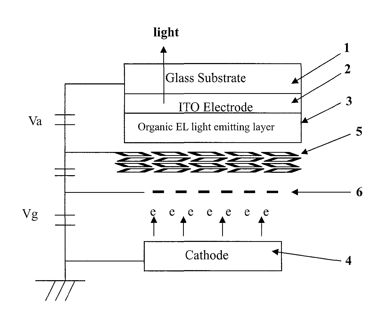
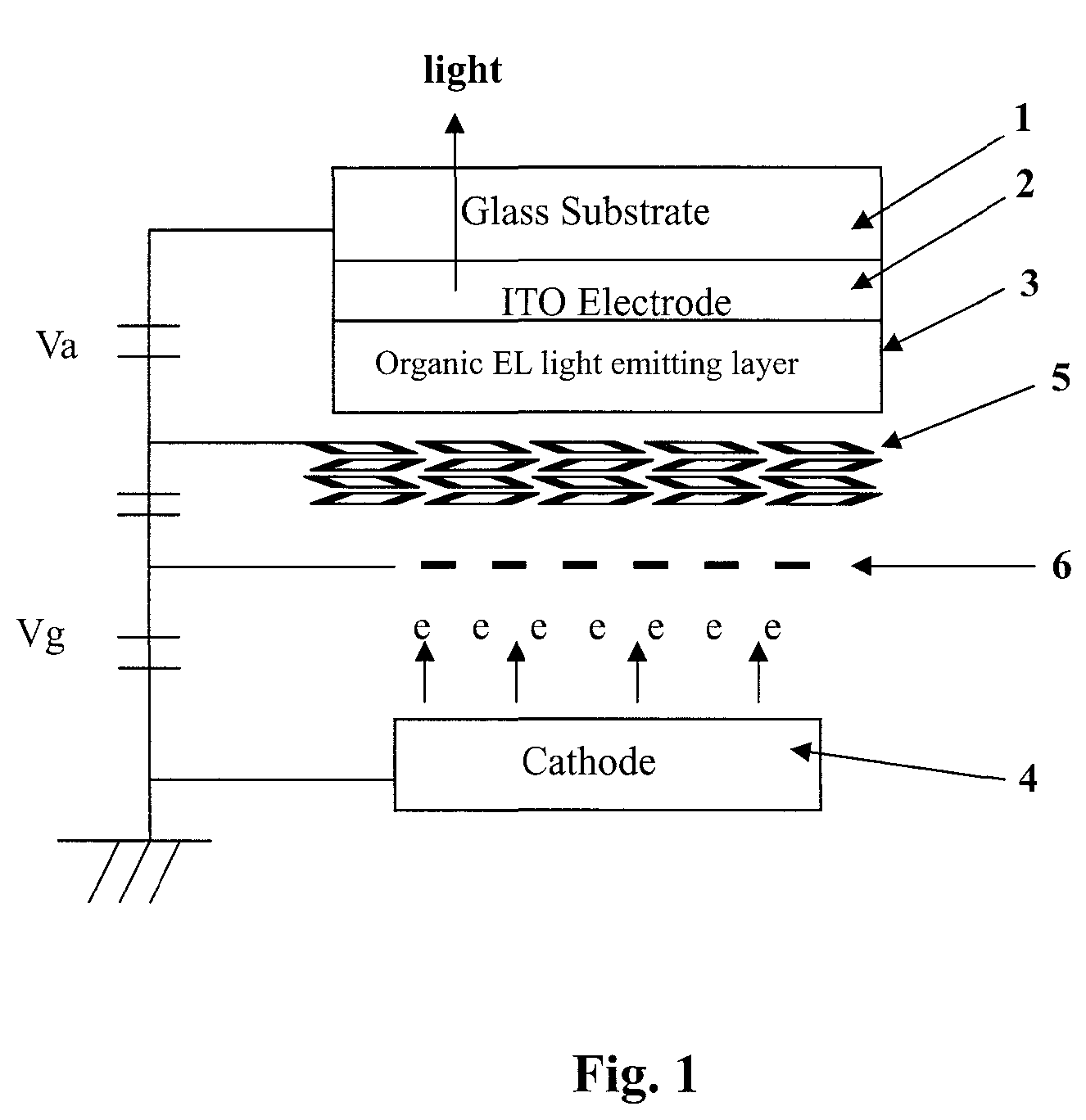
[0035]As the electron source, the cathode 4 can be made of low work function metal such as tungsten, or implemented with a cold electron source cathode of the CNT, Spindt, PN, MIM, or surface emission types.

[0036]Refer to FIG. 1, the dynode 5 can be of the metal channel, box, line focus, mesh, or MPC types as shown in FIGS. 10-14.

[0037]The secondary electron material in the dynode 5 can be Cu—Be or Ag—Mg alloys. The secondary electron material coating on the organic EL light emitting layer 3 can be metal oxide of Be, Mg, or Ca.

[0038]This...

third embodiment

[0051]FIG. 8 shows the FEOLED device of the present invention in which the dynode is omitted. In such case, the secondary electron material, which can be made of oxides of Be, Mg, or Ca, is coated directly on the organic EL light emitting layer 3.

[0052]Refer to FIG. 9, in designs in which the dynode 5 is absent, a metal back 10 can be grown on the organic EL light emitting layer 3. This metal back 10 interfaces the organic EL light emitting layer 3 to the cathode 4, as well as prevents damages caused when electrons are injected to the organic EL light emitting layer 3. The metal back 10 can be made of Cu—Be, Ag—Mg, or Au—Ca alloys. In such configuration, a bias voltage VELth (Vth=threshold voltage for electroluminescence) is first applied between the ITO anode electrode 2 and the metal back 10. Subsequently, the aforementioned secondary electron materials, such as oxides of Be, Mg, or Ca, can be grown between the organic EL light emitting layer 3 and the metal back 10. The combined ...


PUM


Abstract

The essential thought of this patent is that organic emission layer is utilized instead of inorganic phosphor thin film in field emission display (FED). The field emission organic light emitting diode (FEOLED) in this invention is configured with an electron multiplier (dynode) between the cathode of FED and the organic emission layer, wherein secondary electron material is coated in the holes of the dynode. The design for the organic emission layer, which includes a hole injection layer (HIL), a hole transport layer (HTL) and an emission layer (EL), is able to attain higher luminance and lower power consumption for the innovative FEOLED than conventional OLED.

Description

BACKGROUND OF THE INVENTION[0001]1. Field of the Invention[0002]This invention relates to an improved design of field emission display (FED) and more particularly to an FED in which the inorganic fluorescent screen is replaced by an organic EL light emitting layer, forming an innovative field emission organic light emitting diode (FEOLED) with improved luminance and lower power consumption.[0003]2. Description of the Related Art[0004]The CRT (cathode-ray tube) is widely employed in TVs and computer terminals. There are three main parts of a CRT: (1) a cathode electrode for hot electron source, (2) a deflection system for deflecting hot electrons injecting from the cathode electrode in perpendicular and horizontal directions to the inorganic phosphor on a fluorescent screen, and (3) an indium tin oxide (ITO) anode electrode on a transparent glass substrate, which ITO anode electrode is coated with inorganic fluorescent screen. Hot electrons generated by applying a high voltage betwee...

Claims


Application Information

Patent Timeline
Patent Type & Authority Patents(United States)
IPC IPC(8): H01J1/62H01J63/04
CPCH01J29/10H01J31/123H01L51/52H01L51/5203H10K59/805H10K50/80H10K50/805
Inventor YOKOYAMA, MEISO
Owner ITC LIMITED
Why Eureka
Try Eureka