
Ultra thin back-illuminated photodiode array fabrication methods

a back-illuminating and photodiode technology, applied in the field of semiconductor photodiodes, can solve the problems of reducing the photodiode performance with respect, limiting the design of the front-illuminating photodiode array, and imposing severe constraints on the metal run width

Inactive Publication Date: 2008-12-09
ARRAY OPTRONIX
View PDF22 Cites 14 Cited by
  • Summary
  • Abstract
  • Description
  • Claims
  • Application Information

AI Technical Summary

Benefits of technology

"The present invention relates to semiconductor photodiodes, and in particular, to the structures of high performance, back-illuminated photodiode arrays and the methods of fabricating such structures. The technical effects of the invention include providing multiple element, backside-illuminated 2D-photodiode arrays with a superior performance of all elements, and providing fabrication methods for the backside-illuminated photodiode array on an ultra thin wafer. These improvements allow for the fabrication of more complex and efficient photodiode arrays with improved performance and reduced cross-talk."

Problems solved by technology

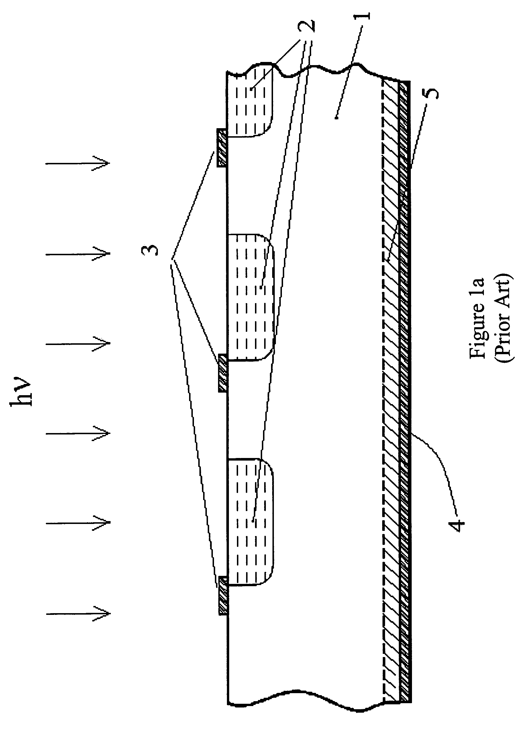
For example, traditional front illuminated structures like that shown in FIG. 1a allow building high performance photodiodes and photodiode arrays, but impose severe constraints on the metal run width.
Those constraints limit a design of the front illuminating photodiode array to the use of either a smaller number of elements, or larger gaps between adjacent elements.
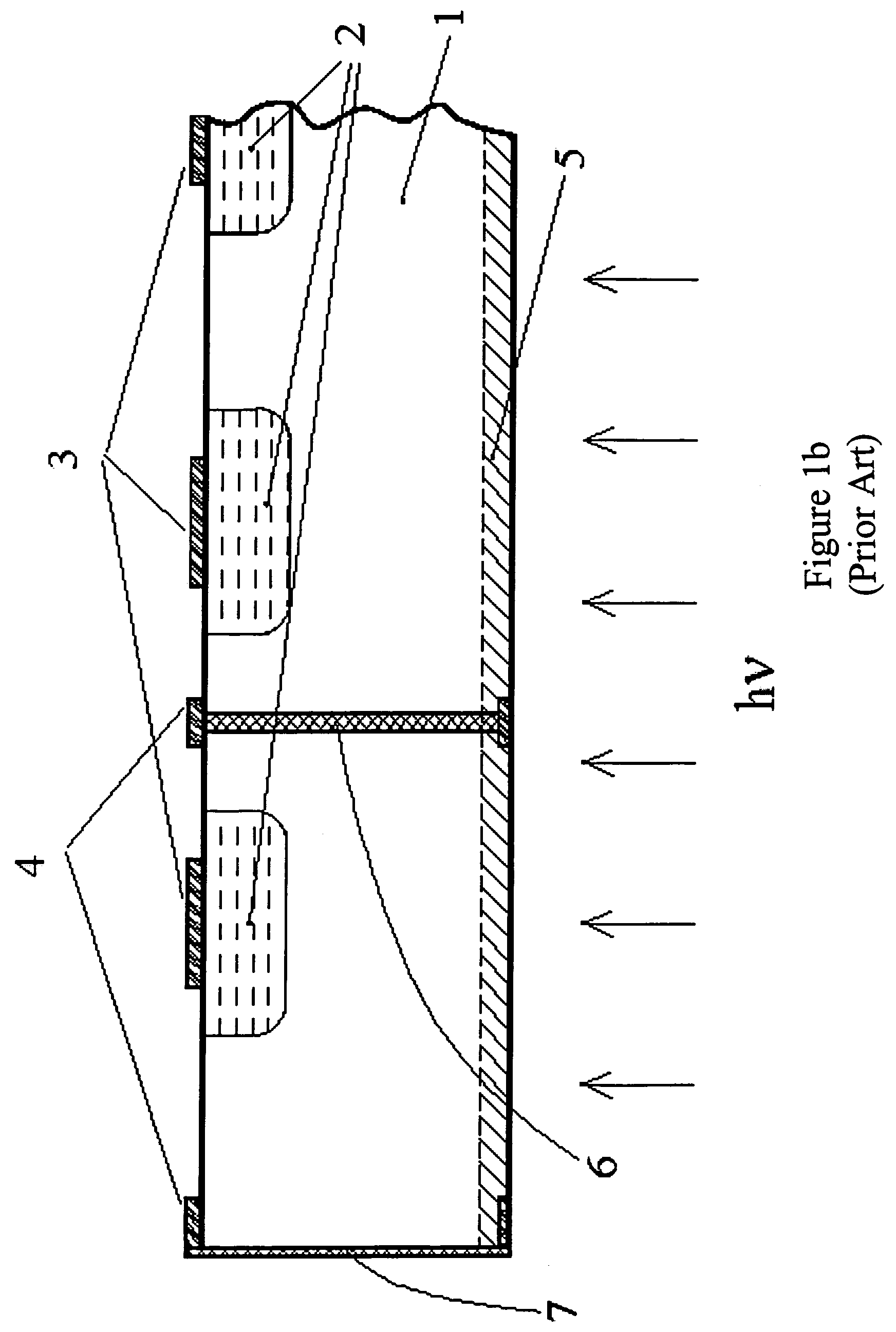
However, several drawbacks of the previously reported back illuminated structures limit their application:1) First, these structures are usually fabricated using relatively thick wafers (>50 μm) and the resistivity of the material has to be high enough (>1000 Ohm-cm) to deplete the entire volume at zero bias, which is required for many applications;2) Second, the application of a high resistivity material usually diminishes the photodiode performance with respect to the leakage current and shunt resistance;3) Third, if a high resistivity material is not used, then the time response will be very long (micro seconds or even longer) because the time response would be determined by the diffusion processes rather than drift processes of the totally depleted structures;4) Fourth, there are little or no structural features that isolate adjacent cells from each other within the entire thickness of the device, which results in relatively high cross-talk, especially at zero bias.

Method used


Image

  • Ultra thin back-illuminated photodiode array fabrication methods
  • Ultra thin back-illuminated photodiode array fabrication methods
  • Ultra thin back-illuminated photodiode array fabrication methods

Examples


Embodiment Construction

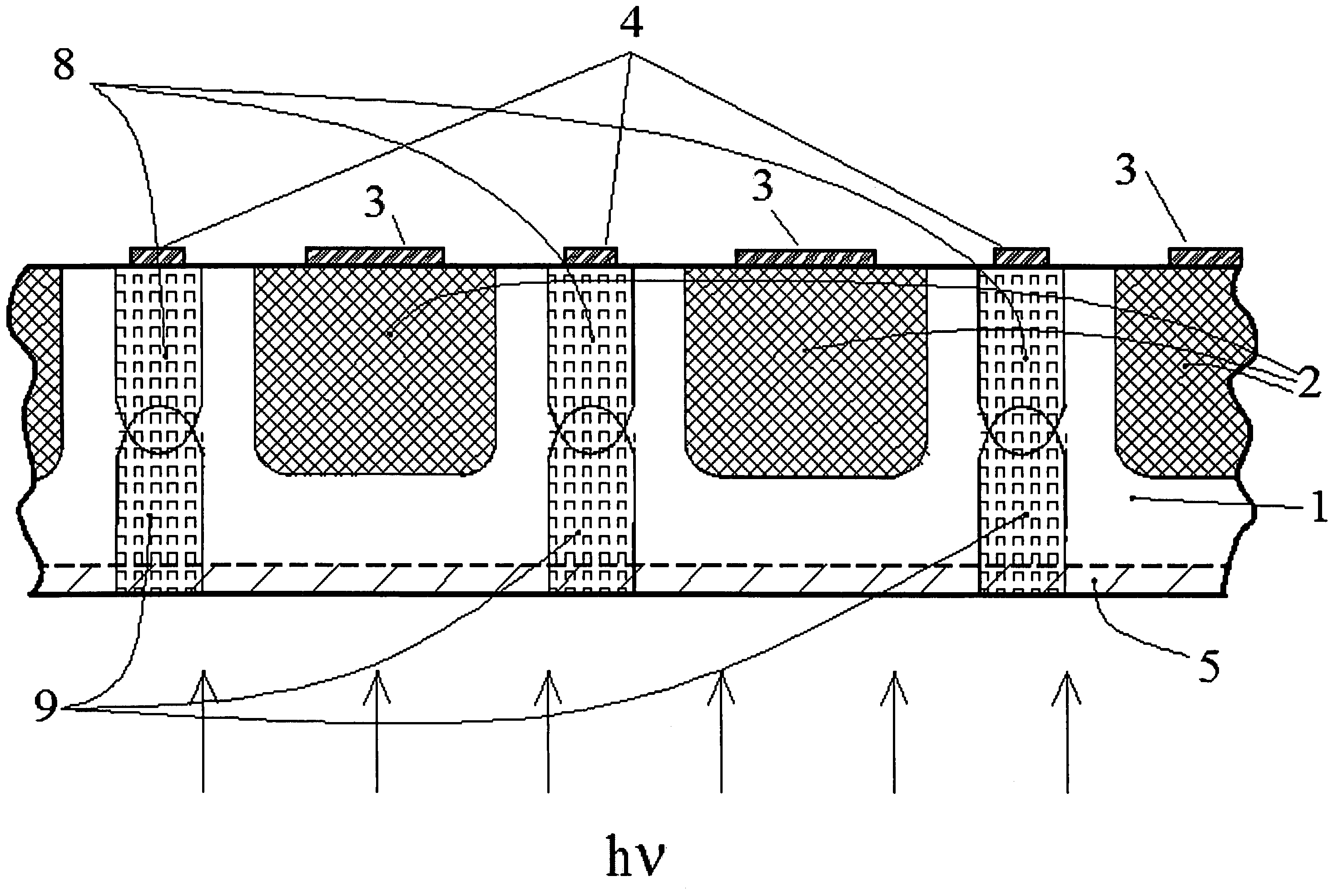
[0018]The objectives of the present invention include:[0019]1) To provide multiple element, backside illuminated 2D-photodiode arrays with a superior performance of all elements;[0020]2) To provide fabrication methods for the backside-illuminated photodiode array on an ultra thin wafer.

[0021]It is therefore an object of this invention to provide a structure for silicon multi-element, 2-D photodiode arrays having greatly improved characteristics over prior art arrays, making it useful in such applications as CT scanner applications, etc.

[0022]Another object is to provide a method of fabricating Si devices on ultra thin wafers, which method can be suitable for fabrication of flip-chip, multi-element, 2-dimensional arrays of silicon photodiodes.

[0023]Another object is to provide a method of handling ultra thin wafers during wafer fabrication, which method should secure ultra thin wafers against accidental breakage, etc.

[0024]These and other objects of the present invention will become ...


PUM

PropertyMeasurementUnit
thicknessaaaaaaaaaa
thicknessaaaaaaaaaa
thicknessaaaaaaaaaa

Abstract

Ultra thin back-illuminated photodiode array fabrication methods providing backside contact by diffused regions extending through the array substrate. In accordance with the methods, a matrix is diffused into one surface of a substrate, and at a later stage of the substrate processing, the substrate is reduced in thickness and a similar matrix is diffused into the substrate from the other side, this second diffusion being aligned with the first and contacting the first within the substrate. These two contacting matrices provide good electrical contact to a conductive diffusion on the backside for a low resistance contact to the backside. Various embodiments are disclosed.

Description

CROSS-REFERENCE TO RELATED APPLICATIONS[0001]This application is a continuation-in-part of U.S. patent application Ser. No. 10 / 863,558 filed Jun. 8, 2004 now U.S. Pat. No. 7,112,465, which is a divisional of U.S. patent application Ser. No. 10 / 606,053, filed Jun. 25, 2003, now U.S. Pat. No. 6,762,473.BACKGROUND OF THE INVENTION[0002]1. Field of the Invention[0003]The present invention relates to semiconductor photodiodes, and in particular, to the structures of high performance, back-illuminated photodiode arrays and the methods of fabricating such structures.[0004]2. Prior Art[0005]Conventional photodiode array structures are based on either front illuminated or back illuminated technologies. FIG. 1a is a simplified cross section of an exemplary prior art front illuminated photodiode array and FIG. 1b is a simplified cross section of an exemplary prior art back illuminated photodiode array. The substrate may be either n-type or p-type material, with opposite conductivity type diffu...

Claims


Application Information

Patent Timeline
Patent Type & Authority Patents(United States)
IPC IPC(8): H01L21/30H01L21/335H01L27/144H01L27/146H01L31/18
CPCH01L27/1446H01L27/14687H01L27/1464H01L31/1804H01L27/14643Y10S438/963Y02E10/547
Inventor METZLER, RICHARD A.GOUSHCHA, ALEXANDER O.
Owner ARRAY OPTRONIX
Learn More