Semiconductor device and method for manufacturing the same

a semiconductor film or insulating film technology, applied in the direction of semiconductor devices, basic electric elements, electrical appliances, etc., can solve the problems of insufficient film quality, risk of leakage current or short circuit between a semiconductor film and a gate electrode, and difficulty in employing thermal oxidation methods, etc., to achieve excellent characteristics and improve the surface quality of the semiconductor film or the insulating film

Inactive Publication Date: 2008-12-16
SEMICON ENERGY LAB CO LTD
View PDF44 Cites 42 Cited by
  • Summary
  • Abstract
  • Description
  • Claims
  • Application Information

AI Technical Summary

Benefits of technology

[0012]A semicondcutor film or an insulating film is oxided or nitrided by a plasma treatment and the surface quality of the semiconductor film or the insulating film is improved, thereby obtaining a dense insulating film. Thus, a semiconductor device having excellent characteristics can be manufactured.

Problems solved by technology

However, an insulating film formed to have a thickness of several nm by a CVD method or a sputtering method has a defect in the film and the film quality is not sufficient.
For example, in a case that an insulating film formed by a CVD method is used as a gate insulating film, there is a risk of leakage current or a short circuit between a semiconductor film and a gate electrode.
In addition, by a thermal oxidation method, for example, a dense insulating film can be formed by oxidizing a surface of the semiconductor film; however, since in manufacturing a thin film transistor, a low heat resistant substrate such as glass is used on the cost front, it is difficult to employ a thermal oxidation method.

Method used


Image

  • Semiconductor device and method for manufacturing the same
  • Semiconductor device and method for manufacturing the same
  • Semiconductor device and method for manufacturing the same

Examples


embodiment mode 1

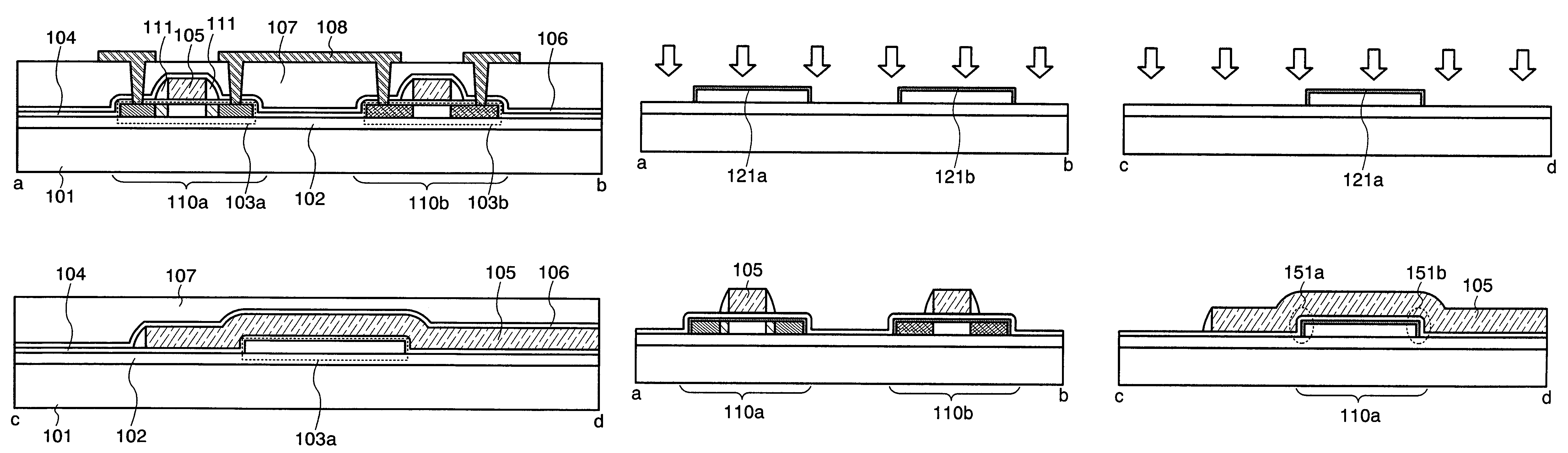
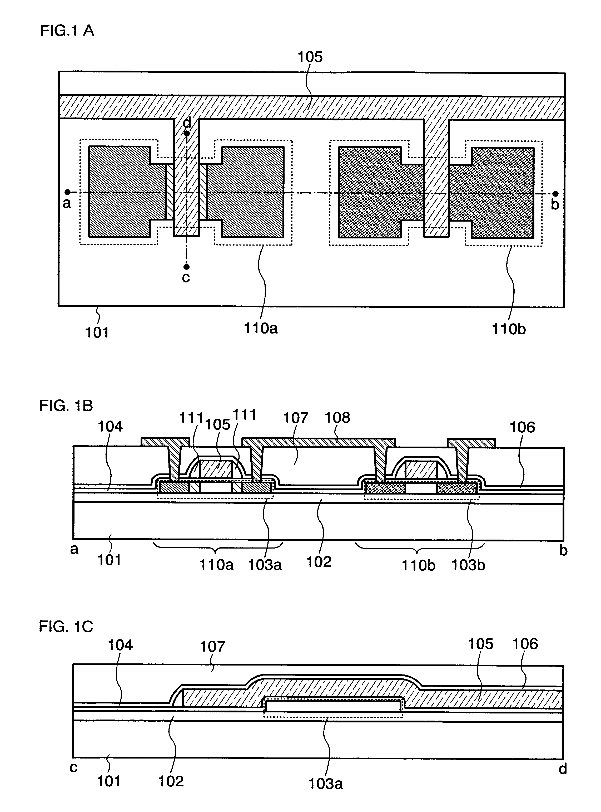
[0056]In Embodiment Mode 1, with reference to drawings, a manufacturing method of a semiconductor device is described, in which a plasma treatment is conducted to the semiconductor films 103a and 103b or the gate insulating film 104 shown in FIGS. 1A to 1C, and an oxidation treatment or a nitriding treatment is conducted to the semiconductor films 103a and 103b or the gate insulating film 104.

[0057]This embodiment mode shows a case that island-shaped semiconductor films are provided over the substrate first, and the shape of an end portion of the island-shaped semiconductor film is generally orthogonal.

[0058]Island-shaped semiconductor films 103a and 103b are formed on a substrate 101 (FIG. 2A). As to the island-shaped semiconductor films 103a and 103b, an amorphous semiconductor film is formed using a material mainly containing silicon (Si) (e.g., SixGe1-x etc.,) over an insulating film 102 which have been formed over the substrate 101, by a sputtering method, an LPCVD method, a pl...

embodiment mode 2

[0099]Embodiment Mode 2 describes a structure of a semiconductor device of the present invention, which is different from that of the described above embodiment mode with reference to drawings.

[0100]In this embodiment mode, a plasma treatment is conducted to the substrate 101 or the insulating film 102 shown in FIGS. 1A to 1C. By oxidizing or nitriding the substrate 101 or the insulating film 102, a semiconductor device is manufactured. The method is described with reference drawings.

[0101]A case is described with reference to drawings, that the substrate 101 is oxidized or nitrided by conducting a plasma treatment to the substrate 101 first.

[0102]The substrate 101 is prepared, and is washed with hydrofluoric acid (HF), alkali or pure water (FIG. 8A). As the substrate 101, a glass substrates such as alumino borosilicate glass or barium borosilicate glass, a quartz substrate, a ceramic substrate, a metal substrate including stainless steel or the like can be used. In addition, a subs...

embodiment mode 3

[0123]Embodiment Mode 3 describes another structure of a semiconductor device of the present invention which is different from those of the above embodiment modes with reference to drawings.

[0124]This embodiment mode describes a case that a plasma treatment is conducted to the insulating film 106 or the insulating film 107 shown in FIGS. 1A to 1C to oxide or nitride the insulating film 106 or the insulating film 107 with reference to drawings.

[0125]Island-shaped semiconductor films 103a and 103b are provided over a substrate 101 with an insulating film 102 interposed therebetween, and a gate electrode 105 is formed over the semiconductor film 103a, 103b with a gate insulating film 104 interposed therebetween, and an insulating film 106 is formed to cover the gate electrode 105 by a sputtering method, an LPCVD method, a plasma CVD method or the like (FIG. 11A).

[0126]Next, a plasma treatment is conducted to oxide or nitride the insulating film 106, and thus, an oxide film or a nitride...


PUM


Abstract

A manufacturing method of a semiconductor device of the present invention includes the steps of forming a first insulating film over a substrate, forming a semiconductor film over the first insulating film, oxidizing or nitriding the semiconductor film by conducting a plasma treatment to the semiconductor film under a condition of an electron density of 1×1011 cm−3 or more and 1×1013 cm−3 or less and an electron temperature of 0.5 eV or more and 1.5 eV or less, using a high frequency wave, forming a second insulating film to cover the semiconductor film, forming a gate electrode over the second insulating film, forming a third insulating film to cover the gate electrode, and forming a conductive film over the third insulating film.

Description

BACKGROUND OF THE INVENTION[0001]1. Field of the Invention[0002]The present invention relates to a semiconductor device having a good-quality film obtained by conducting a plasma treatment to an insulating film or a semiconductor film to improve the quality of the surface, in a case that a conductive film, the insulating film, the semiconductor film and / or the like are / is stacked, and a manufacturing method thereof.[0003]2. Description of the Related Art[0004]In recent years, a technique for forming a thin film transistor (TFT) having a semiconductor thin film (the thickness of several nm to several hundreds nm) formed over a substrate having an insulating surface such as glass has been attracted. Such thin film transistors have been widely applied to semiconductor devices such as ICs or electro optical devices, and further, such thin film transistors have been needed to have a more miniaturized structure, in response to demands for downsizing and high performance of the semiconduct...

Claims


Application Information

Patent Timeline
Patent Type & Authority Patents(United States)
IPC IPC(8): H01L21/31H01L21/469
CPCH01L27/12H01L27/1248H01L29/66757H01L29/42384H01L21/3065
Inventor ISOBE, ATSUOMURAKAMI, SATOSHITAKANO, TAMAEYAMAZAKI, SHUNPEI
Owner SEMICON ENERGY LAB CO LTD
Why Eureka
Try Eureka