OLED device having improved output and contrast with light-scattering layer and contrast-enhancement layer

a technology of light scattering layer and oled device, which is applied in the direction of discharge tube/lamp details, discharge tube luminescnet screen, incadescent envelope/vessel, etc., can solve the problems of reducing the image quality oled devices generally suffer from poor ambient contrast, and can absorb as much as 40% of the emitted light, so as to improve the light efficiency and ambient contrast of the oled device

Active Publication Date: 2008-12-16
GLOBAL OLED TECH
View PDF19 Cites 97 Cited by
  • Summary
  • Abstract
  • Description
  • Claims
  • Application Information

AI Technical Summary

Problems solved by technology

However, OLED devices generally suffer from poor ambient contrast because of the reflectivity of the reflective electrode.
Such a reflector tends to reflect ambient light thus reducing the contrast between the emitted light and the ambient light and decreasing the image quality of the OLED device.
However, such polarizers are expensive and also absorb as much as 40% of the emitted light.
Such louver films are typically employed on the top surface of a display device, and while effective at reducing viewing angles, typically have not been suggested for use in displays with improved light output and sharpness of display images.
It has also been found, that one of the key factors that limits the efficiency of OLED devices is the inefficiency in extracting the photons generated by the electron-hole recombination out of the OLED devices.
Due to the high optical indices of the organic materials used, most of the photons generated by the recombination process are actually trapped in the devices due to total internal reflection.
In general, up to 80% of the light may be lost in this manner.
In any of these OLED structures, the problem of trapped emitted light and reflected ambient light remains.
Moreover, the contrast of the device is not improved under diffuse illumination.
Moreover, trapped light may propagate a considerable distance horizontally through the cover, substrate, or organic layers before being scattered out of the device, thereby reducing the sharpness of the device in pixellated applications such as displays.
The particular arrangements, however, may still result in reduced sharpness of the device and does not improve contrast.
Such disclosed designs, however, do not improve the contrast of the device.
While such methods are useful, the presence of a reflective electrode still decreases the ambient contrast significantly.
As noted above, circular polarizers may be employed, but applicants have determined that light-extraction techniques such as scattering layers tend to be incompatible with such polarizers.

Method used


Image

  • OLED device having improved output and contrast with light-scattering layer and contrast-enhancement layer
  • OLED device having improved output and contrast with light-scattering layer and contrast-enhancement layer
  • OLED device having improved output and contrast with light-scattering layer and contrast-enhancement layer

Examples


Embodiment Construction

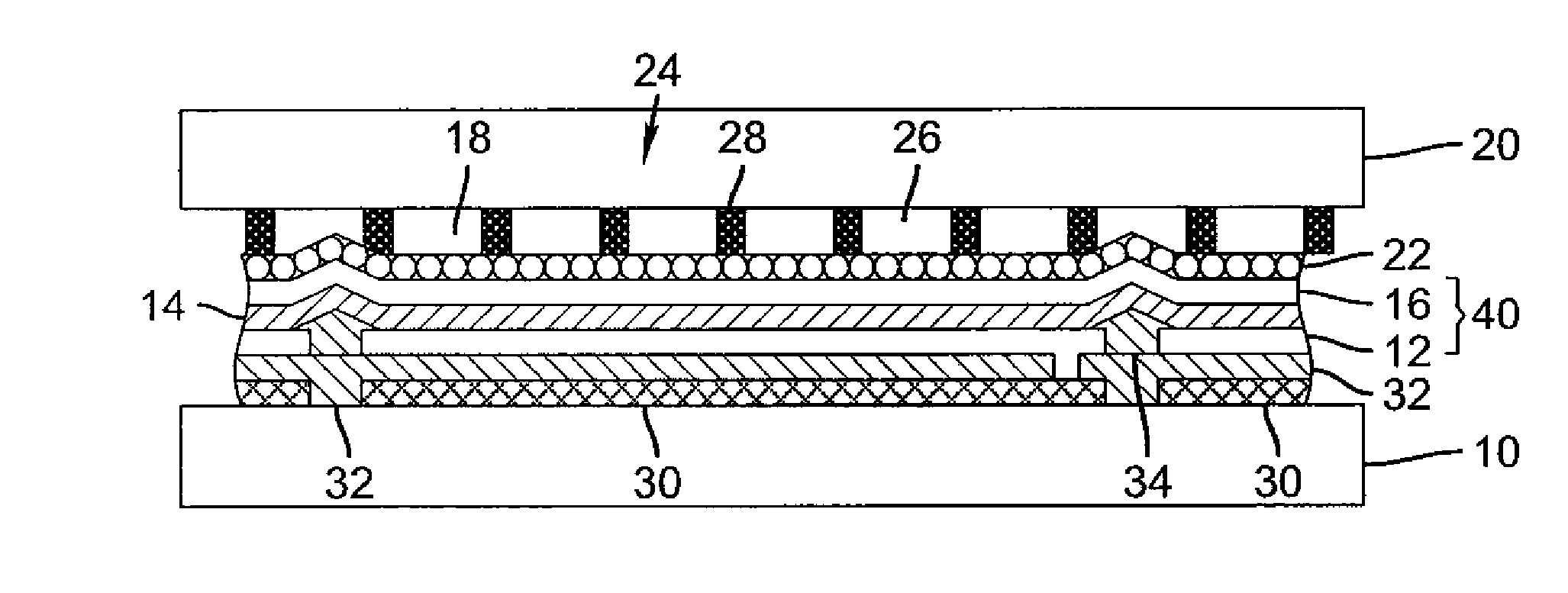
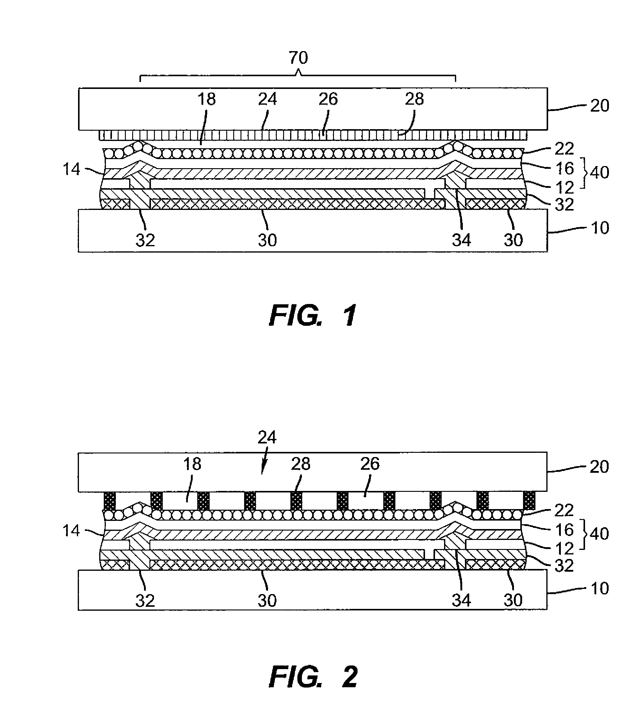
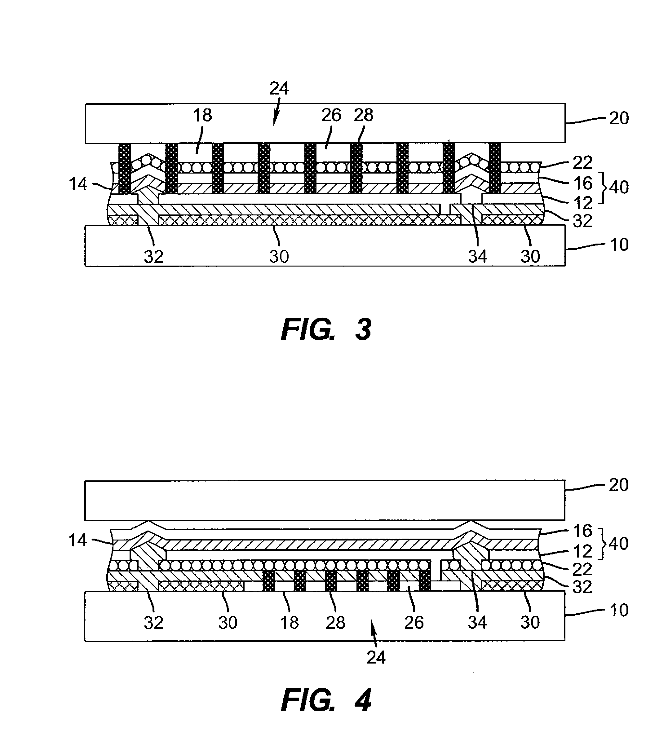
[0036]Referring to FIG. 1, in accordance with one embodiment of the present invention, an organic light-emitting diode (OLED) device, comprises an OLED 40 formed over a substrate 10 having a first patterned electrode 12 defining independently controllable light-emitting areas 70, and a transparent second electrode 16 formed over the first electrode, wherein one or more layers 14 of light-emitting organic material are formed between the electrodes 12 and 16, the organic material layer(s) 14 having a first optical index. A transparent cover 20 is formed over the OLED 40 and has a second optical index, and light is emitted through the transparent cover 20. A light-scattering layer 22 is formed between the cover 20 and substrate 10 for scattering light. A low-index element 18 having an optical index lower than the first and second optical indices is formed between the scattering layer 22 and the transparent cover 20. A contrast-enhancement layer 24 comprising a plurality of alternating ...


PUM


Abstract

An organic light-emitting diode (OLED) device, with an OLED formed on a substrate having a first and second electrodes and one or more light-emitting organic material layers formed between the electrodes, the organic material layer(s) having a first optical index and at least one of the electrodes patterned to define light-emitting areas; a cover formed over the OLED. The cover or substrate is transparent and has a second optical index and the light is emitted through the transparent cover or substrate; a light-scattering layer formed between the cover and substrate for scattering light; a low-index element having an optical index lower than the first and second optical indices formed between the scattering layer and the transparent cover or substrate; and a contrast-enhancement layer having a plurality of alternating light-absorbing portions and light-transmissive portions formed in the layer located between the light-scattering layer and the transparent substrate or cover through which light is emitted, wherein a plurality of light-absorbing portions and light-transmissive portions are located in each light-emitting area.

Description

FIELD OF THE INVENTION[0001]The present invention relates to organic light-emitting diode (OLED) devices, and more particularly, to OLED device structures for improving light output and contrast.BACKGROUND OF THE INVENTION[0002]Organic light-emitting diodes (OLEDs) are a promising technology for flat-panel displays and area illumination lamps. The technology relies upon thin-film layers of organic materials coated upon a substrate. OLED devices generally can have two formats known as small molecule devices such as disclosed in U.S. Pat. No. 4,476,292 and polymer OLED devices such as disclosed in U.S. Pat. No. 5,247,190. Either type of OLED device may include, in sequence, an anode, an organic EL element, and a cathode. In most designs, one of the electrodes is reflective and the other transparent. The organic EL element disposed between the anode and the cathode commonly includes an organic hole-transporting layer (HTL), a light-emissive layer (LEL), and an organic electron-transpor...

Claims


Application Information

Patent Timeline
Patent Type & Authority Patents(United States)
IPC IPC(8): H01J1/62
CPCH01L51/5268H01L51/5284H10K50/854H10K50/865
Inventor COK, RONALD S.TUTT, LEE W.
Owner GLOBAL OLED TECH
Why Eureka
Try Eureka