Semiconductor light emitting device and method for manufacturing the same

a technology of semiconductors and light emitting devices, which is applied in the direction of semiconductor devices, basic electric elements, electrical equipment, etc., can solve the problems of low productivity, high manufacturing cost of structure fabrication, and insufficient effect of structur

Inactive Publication Date: 2009-01-13
KK TOSHIBA
View PDF11 Cites 49 Cited by
  • Summary
  • Abstract
  • Description
  • Claims
  • Application Information

AI Technical Summary

Problems solved by technology

Consequently, the structure has not produced sufficient effects.
Thus, the fabrication of the structure requires high manufacturing costs and has a low productivity.
Therefore, the structure is not practical.
However, these methods are susceptible to the crystal face of the substrate.
Thus, the light extracted surface cannot be always roughened, thus limiting the improvement of the light extraction efficiency.
Further, the shape of the concaves and convexes significantly affects the light extraction efficiency.
However, sufficient effects have not been obtained because optimum shapes of the concave and convex structures were unknown.
Furthermore, it is very difficult to highly reproducibly form fine concave and convex structures on the surface of the light emitting surface.

Method used


Image

  • Semiconductor light emitting device and method for manufacturing the same
  • Semiconductor light emitting device and method for manufacturing the same
  • Semiconductor light emitting device and method for manufacturing the same

Examples


example 1

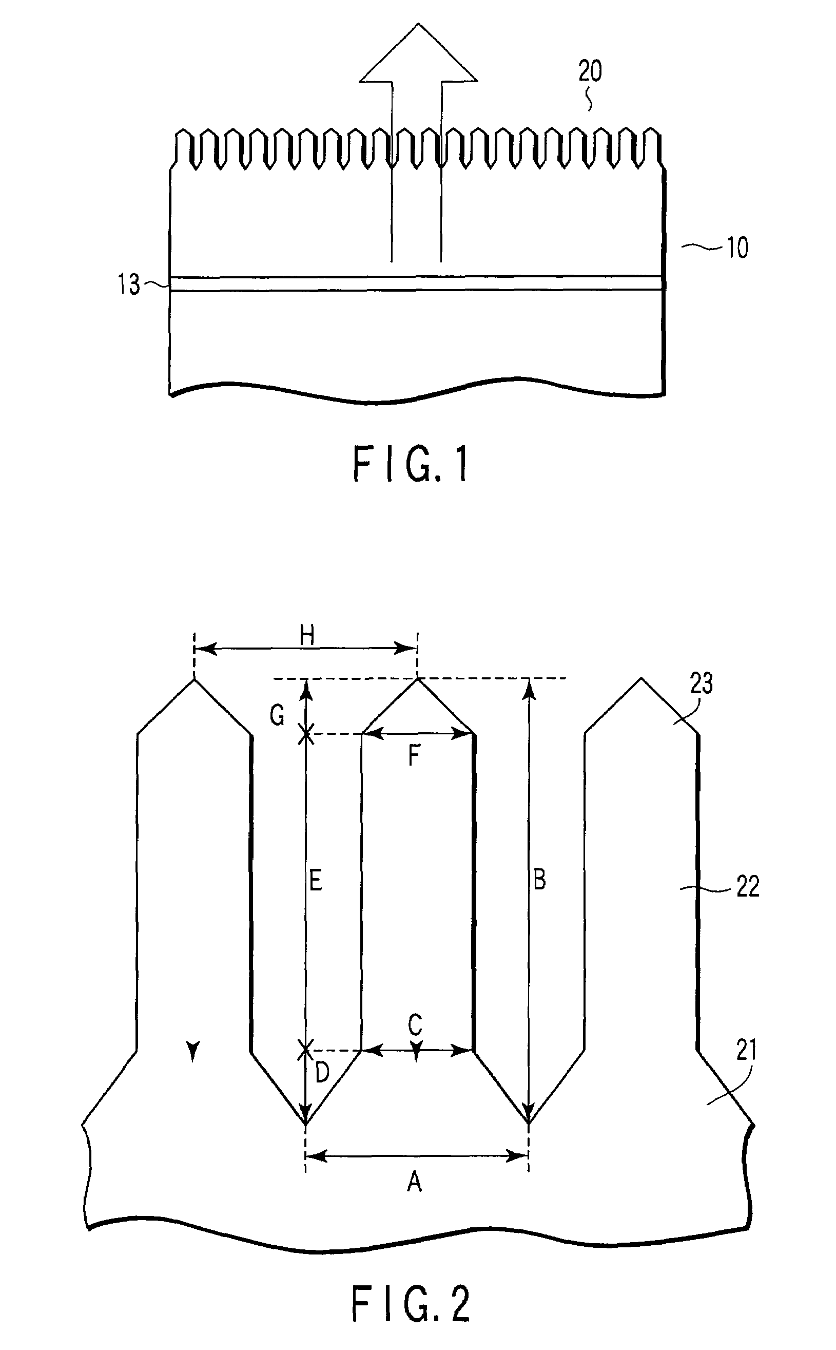
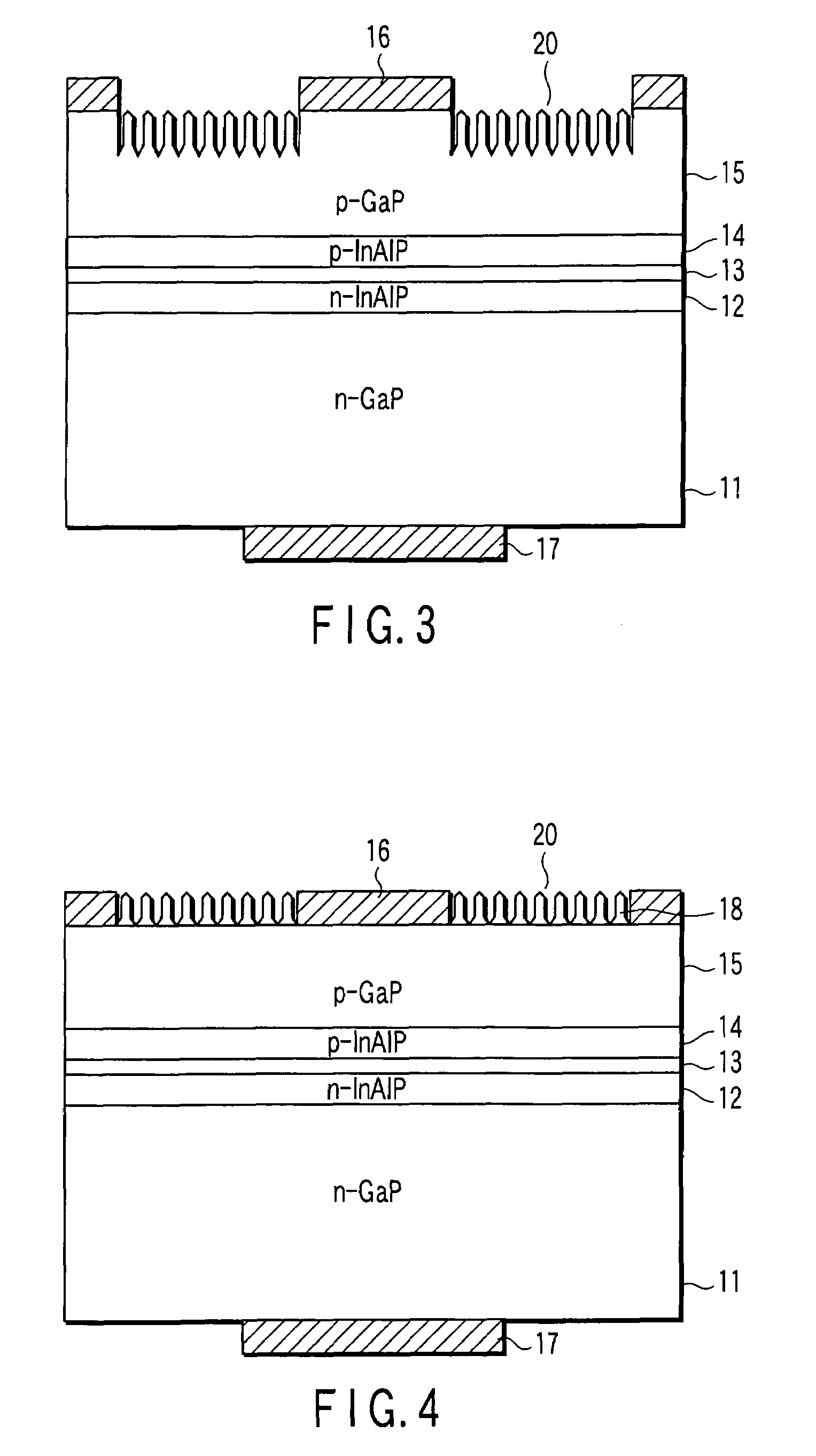
[0109]FIG. 3 is a sectional view showing the element structure of a light emitting diode according to a first example of the present invention.

[0110]A double hetero structure is formed on the n-GaP substrate 11; the double hetero structure has the InGaAlP active layer 13 sandwiched between the n-InAlP clad layer 12 and the p-InAlP clad layer 14. The GaP current diffusion layer 15 is formed on the double hetero structure. The p-side electrode 16 is formed on a part of the p-GaP current diffusion layer 15. The n-side electrode 17 is formed on a part of the bottom surface of the n-GaP substrate 11. Thus, a light emitting diode of emitting wavelength 650 nm is formed.

[0111]In this case, instead of GaP, GaAs may be used as the substrate 11. Instead of GaP, InAlP or InGaAlP may be used as the current diffusion layer 15. Of course, the substrate may be of the p type and the entire conductivity type may be reversed.

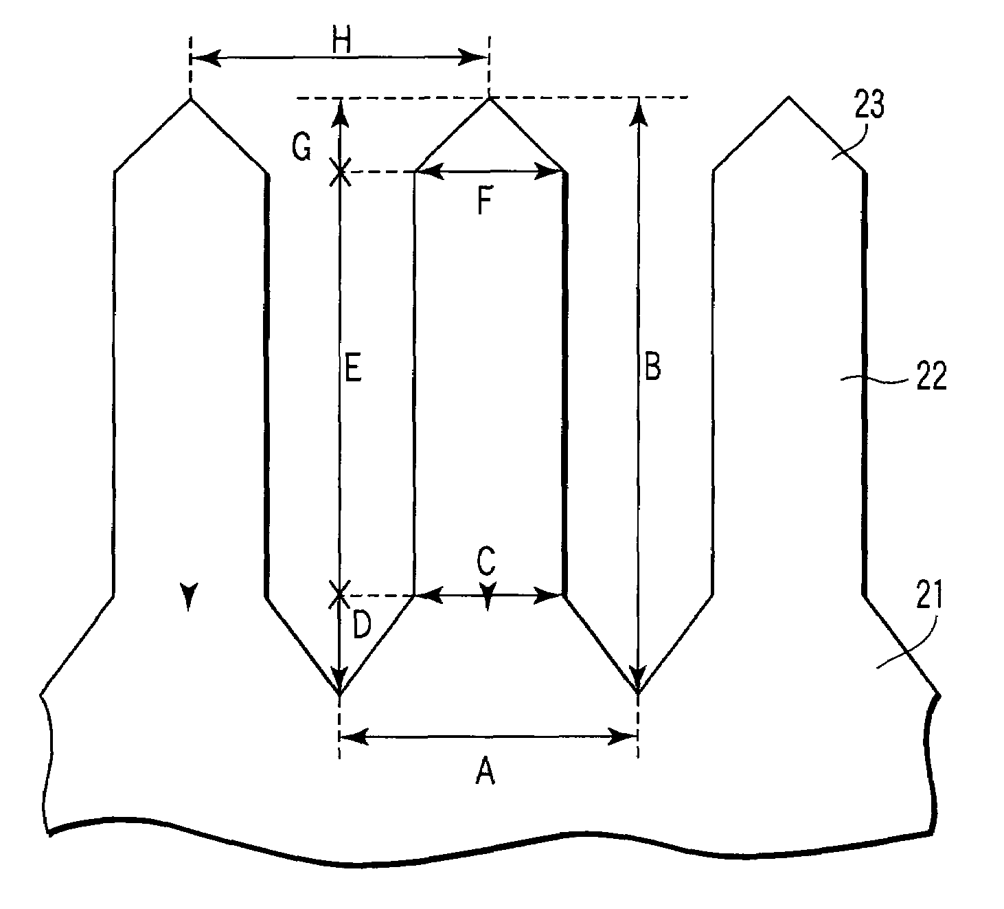
[0112]The convex structures 20, characteristic of the present example, are f...

example 2

[0121]A phase-separated substrate with a block copolymer produced as described in Example 1 was dry etched by RIE at an O2 flow rate of 30 sccm, a pressure of 13.3 Pa (100 mTorr), and a power of 100 W to etch PS and PMMA, separated from each other. O2 etching cannot etch the substrate in contrast to CF4 etching but can selectively etch PMMA. Subsequently, by a process similar to that in Example 1 fine concaves and convexes having conical, cylindrical, and mesa portions was formed.

[0122]On this occasion, the average diameter of the bottom of the mesa portion 21 was 160 nm. The average diameter of the top of the mesa portion 21 was 100 nm. The average height of the mesa portion 21 was 70 nm. The average diameter of the cylindrical portion 22 was 100 nm. The average height of the cylindrical portion 22 was 250 nm. The average diameter of the conical portion 23 was 100 nm. The average height of the conical portion 23 was 80 nm. The period between the convex structures was 180 nm.

[0123]A...

example 3

[0124]The spin coat method was used to coat a solution, at 3,000 rpm, on the current diffusion layer 15, the uppermost layer of the light emitting element formation substrate 10, used in Example 1; the solution was obtained by dissolving a block copolymer containing PS of molecular weight 315,000 and PMMA of molecular weight 785,000. Subsequently, the light emitting element substrate 10 was pre-baked at 110° C. for 90 seconds to vaporize the solvent. A thickness of 150 nm was thus obtained. Then, in a nitrogen atmosphere, the block copolymer film was annealed at 210° C. for four hours to separate PS from PMMA. A PS dot pattern of diameter about 110 nm was formed.

[0125]The phase-separated GaP substrate with the block copolymer was dry etched by RIE at an O2 flow rate of 30 sccm, a pressure of 13.3 Pa (100 mTorr), and a power of 100 W to etch PS and PMMA, separated from each other. O2 etching cannot etch the substrate but can selectively etch PMMA. Since the etching rate ratio of PS t...


PUM


Abstract

In a semiconductor light emitting device, a semiconductor light emitting element has a light extracted surface on which a plurality of convex structures is formed. The convex structures each have a conical mesa portion constituting a refractive index gradient structure, a cylindrical portion constituting a diffraction grating structure, and a conical portion constituting a refractive index gradient structure. The mesa portion, cylindrical portion, and conical portion are arranged in this order from the light extracted surface. The period between the convex structures is longer than 1 / (the refractive index of an external medium+the refractive index of the convex structures) of an emission wavelength and equal to or shorter than the emission wavelength. The circle-equivalent average diameter of the cylindrical portion is ⅓ to 9 / 10 of that of the bottom of the mesa portion.

Description

CROSS-REFERENCE TO RELATED APPLICATIONS[0001]This application is based upon and claims the benefit of priority from prior Japanese Patent Application No. 2004-263741, filed Sep. 10, 2004, the entire contents of which are incorporated herein by reference.BACKGROUND OF THE INVENTION[0002]1. Field of the Invention[0003]The present invention relates to a semiconductor light emitting device such as a light emitting diode or a semiconductor laser, and in particular, to a semiconductor light emitting device having an improved light extraction efficiency, and a method for manufacturing the semiconductor light emitting device.[0004]2. Description of the Related Art[0005]In order to improve the light extraction efficiency of a semiconductor light emitting device, attempts have been made to form a regular structure (concaves and convexes) of a nanometer size on a front surface of the light emitting device (Applied Physics Letters, 142, vol. 78, 2001, Jpn. J. Appl. Phys., L735, vol 139, 2000). ...

Claims


Application Information

Patent Timeline
Patent Type & Authority Patents(United States)
IPC IPC(8): H01L29/06H01L33/22
CPCH01L33/22
Inventor FUJIMOTO, AKIRAASAKAWA, KOJIOHASHI, KENICHI
Owner KK TOSHIBA
Why Eureka
Try Eureka