

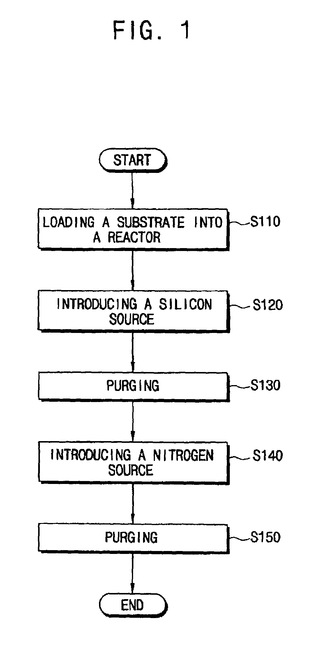
Methods of forming silicon nitride layers using nitrogenous compositions
a technology of nitrogen composition and silicon nitride, which is applied in the direction of hydrogen production, coatings, chemistry apparatus and processes, etc., can solve the problems of conductive structures of semiconductor devices that may show a greater extent of deterioration, silicon wafers may exhibit thermal damage, and impurities diffused from silicon wafers
Active Publication Date: 2009-02-10
SAMSUNG ELECTRONICS CO LTD
View PDF13 Cites 55 Cited by
- Summary
- Abstract
- Description
- Claims
- Application Information
AI Technical Summary
Benefits of technology
The present invention provides nitrogenous compositions for forming a silicon nitride layer at a low temperature with desirable characteristics. The nitrogenous composition includes a hydrazine compound, an amine compound or a mixture thereof, and a silicon source including hexachlorodisilane. The invention also provides methods for forming silicon nitride layers by introducing a silicon source into a reactor to chemically react with a surface of a substrate, introducing a purge gas to remove unreacted silicon source and nitrogenous composition, and introducing a second purge gas to remove unreacted nitrogenous composition.
Problems solved by technology
However, because a silicon wafer upon which the silicon nitride layer is formed may be exposed to a high temperature of above about 700° C. for a specified period of time, the silicon wafer may exhibit thermal damage in which impurities are diffused from the silicon wafer.
As a result, a semiconductor device formed on the silicon wafer may have undesirable electrical characteristics, and conductive structures of the semiconductor device may show a greater extent of deterioration.
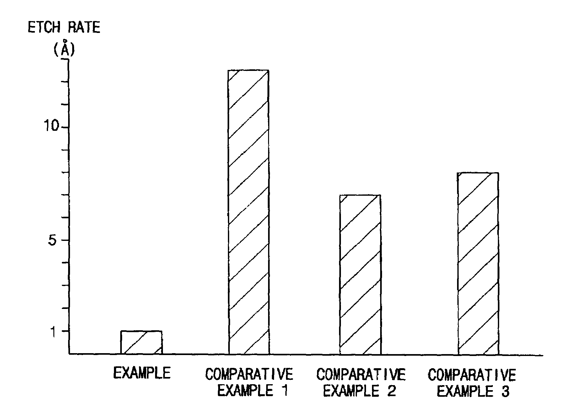
When a silicon nitride layer is formed at a low temperature of below about 600° C. using hexachlorodisilane and ammonia, the silicon nitride layer may not possess a dense structure, and the silicon nitride layer may possess a high etching rate because, for instance, ammonia may not be easily dissociated at the low temperature.
Since the silicon nitride layer may exhibit a high etching rate with respect to an etching solution for etching a nitride layer, the silicon nitride layer may not be employed as an etch stop layer or a hard mask layer in a semiconductor device.
Additionally, because the silicon nitride layer may have undesirable electrical characteristics such as a low breakdown voltage, the semiconductor device including the silicon nitride layer may also have undesirable electrical characteristics.
Although the above-mentioned methods use a nitrogen source for forming a nitride layer, a silicon source is not considered in the formation of a silicon nitride layer.
Method used
View moreImage
Smart ImageViewing Examples

Examples
example
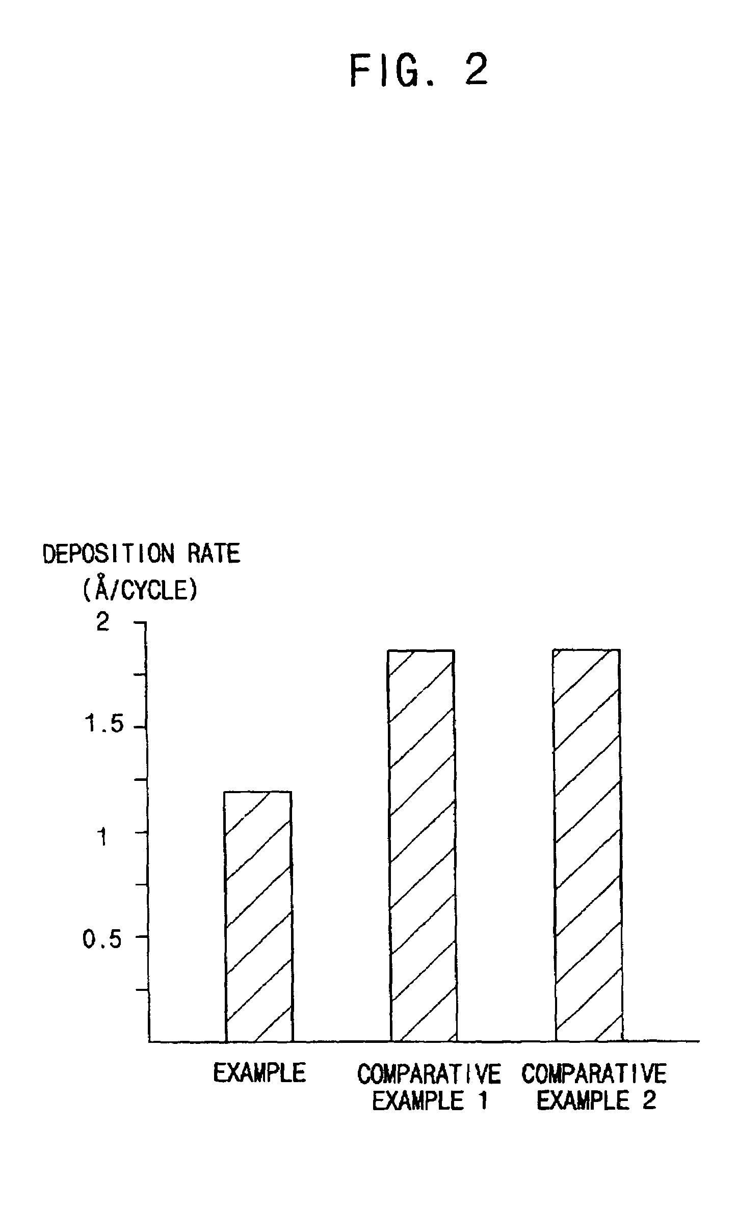
[0046]A silicon nitride layer was formed on a substrate using a silicon source including hexachlorodisilane (HCD) and a nitrogen source including tertiary-butyl-amine (tert-BuNH2:(CH3)3CNH2). The silicon nitride layer was formed at a temperature of about 570° C. in an atomic layer deposition chamber.
Login to View More PUM
| Property | Measurement | Unit |
|---|---|---|
| refractive index | aaaaa | aaaaa |
| temperature | aaaaa | aaaaa |
| temperature | aaaaa | aaaaa |
Abstract
The present invention provides nitrogenous compositions for forming a silicon nitride layer, wherein the nitrogenous composition comprises a hydrazine compound, an amine compound or a mixture thereof. The present invention further provides source compositions for forming a silicon nitride layer, wherein the source composition comprises a nitrogenous composition comprising a hydrazine compound, an amine compound or a mixture thereof, and a silicon source comprising hexachlorodisilane. Methods for forming silicon nitride layers are further provided. The silicon nitride layers provided herein may be formed on a substrate at a low temperature and may further exhibit improved breakdown voltage and an enhanced etch resistance.
Description
RELATED APPLICATION[0001]This application claims the benefit under 35 U.S.C. § 119 to Korean Patent Application No. 2004-1117, filed on Jan. 8, 2004, the disclosure of which is incorporated herein by reference in its entirety as if set forth fully herein.FIELD OF THE INVENTION[0002]The present invention relates to nitrogenous compositions that may be used as a source for forming silicon nitride layers, and methods for forming silicon nitride layers using the nitrogenous compositions. More particularly, the present invention relates to nitrogenous compositions including a hydrazine compound, an amine compound or a mixture thereof for forming at a low temperature a dense silicon nitride layer having desirable characteristics, and methods for forming such silicon nitride layers using the nitrogenous compositions.BACKGROUND OF THE INVENTION[0003]In general processes for manufacturing a semiconductor device, a nitride layer may be used as a hard mask, a spacer, an etch-stop layer, and th...
Claims
Login to View More Application Information
Patent Timeline
 Patent Type & AuthorityPatents(United States)
IPC IPC(8): H01L21/44C01B21/00C23C16/34C23C16/455H01L21/314H01L21/318
CPCC23C16/345C23C16/45553H01L21/3141H01L21/3185H01L21/02271H01L21/0228H01L21/0217H01L21/02274H01L21/02211D06M15/233D06M15/263D06M11/45D06M15/53D06M15/643
InventorKIM, JIN-GYUNAHN, JAE-YOUNGKIM, HEE-SEOKLIM, JU-WAN
OwnerSAMSUNG ELECTRONICS CO LTD