Surface micro sensor and method

Inactive Publication Date: 2009-02-10
ENVIRONMENTAL METROLOGY CORP
View PDF8 Cites 13 Cited by
  • Summary
  • Abstract
  • Description
  • Claims
  • Application Information

AI Technical Summary

Benefits of technology

[0013]The present invention provides a micro sensor for monitoring the cleaning and drying processes of surfaces of dielectric films, micro features in porous dielectric films and biologic or other cells common in microelectronics fabrication, MEMS fabrication or microbiology test system fabrication. By embedding electrodes in the surface of a supporting dielectric, the sensor can probe the surface and pores of a covering dielectric or a cell on the covering dielectric. The addition of a guard reduces the effects of any parasitic capacitance, which extends the measurement bandwidth of the sensor and allows it to be manufactured at the scale of a single cell, a feature that is particularly important for applications in microbiology.
[0015]In another embodiment, the micro sensor is configured with a guard that reduces the effects of any parasitic capacitance. Electrical connectors are embedded in the supporting dielectric beneath the electrodes to carry the ac measurement signal to the electrodes. These connectors have parasitic capacitances to both the substrate below and fluid above. Conductive guards are embedded in the supporting dielectric and buffered so that their voltages closely track the electrode voltages to shield the connectors from the surrounding environment and thereby reduce the loss of measurement signal through the parasitic capacitance associated with the connectors. The guards suitably comprise conductive layers that lie below the connector to reduce the parasitic capacitance to the substrate and above the connector to reduce the parasitic capacitance to the fluid.

Problems solved by technology

A major challenge in manufacturing of the micro and nano devices is the cleaning and drying of very small “micro features”.
Cleaning and drying occur repeatedly during the processing chain and are responsible for a significant part of the total processing time and for the consumption of much of the water, chemicals and energy.
Improper cleaning and drying would have a significant effect on manufacturing yield and device performance and reliability in both semiconductor and MEMS fabrication.
Over-cleaning, over-rinsing or over-drying results in excessive use of chemicals, water and energy and also increases cycle time and potentially causes yield loss.
The key reason for this inefficient and costly approach is that no sensors or techniques are available to measure the cleanliness and monitor the removal of impurities from micro features—to measure cleanliness where it actually counts.
The present monitoring techniques and devices do not provide realistic and accurate information on the cleanliness and condition of micro features.
This results in wasted chemicals, increased process time, lowered throughput, increased cost, and it causes reliability issues because of lack of process control.
If the parasitic capacitance dominates the total electrical response, then the circuit will not have a good signal to noise ratio and the sensor will not be very sensitive.
The full ionic concentration range was not experimentally resolvable in comparison to electronic noise.
Romero's trench device does not address in-situ monitoring of dielectric surfaces and does resolve the problem of parasitic capacitance.

Method used


Image

  • Surface micro sensor and method
  • Surface micro sensor and method
  • Surface micro sensor and method

Examples


Embodiment Construction

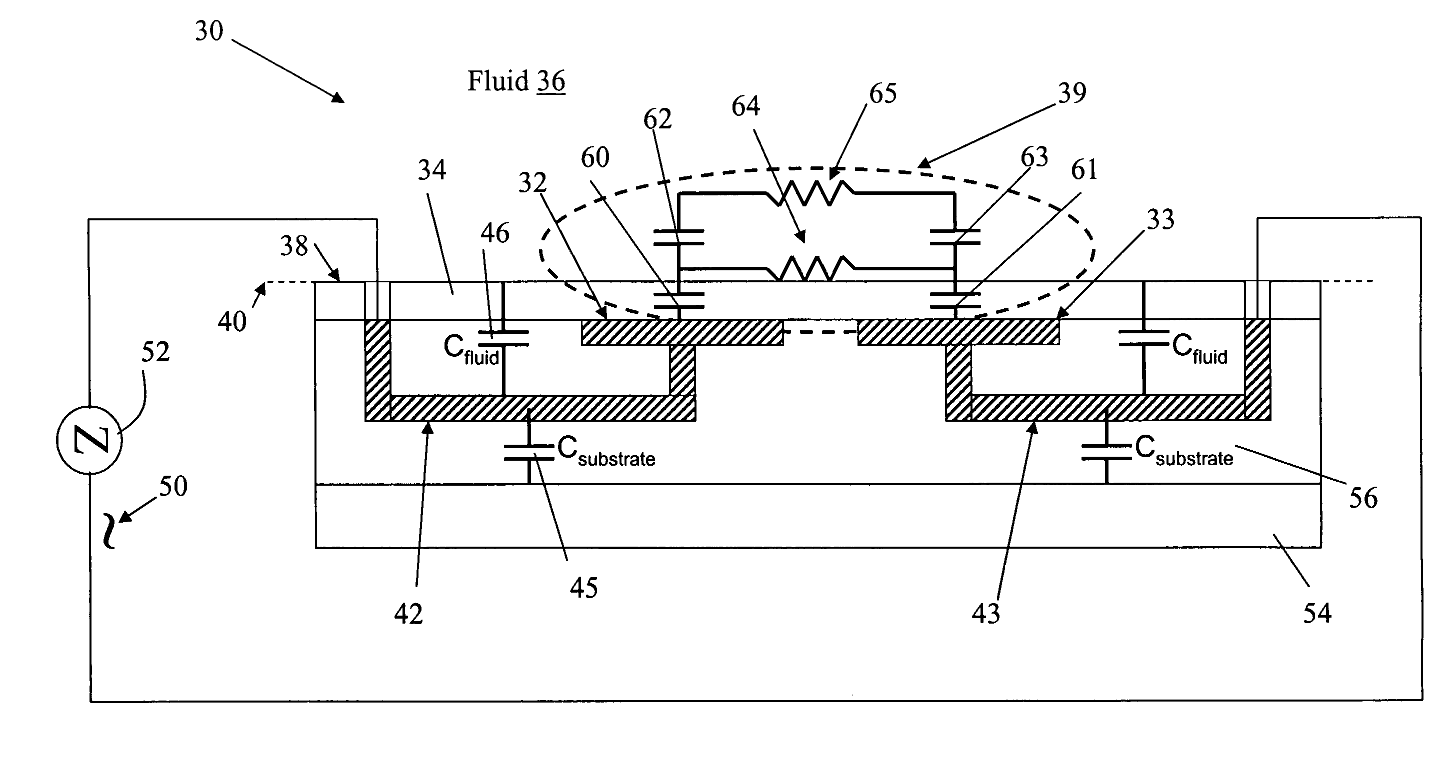
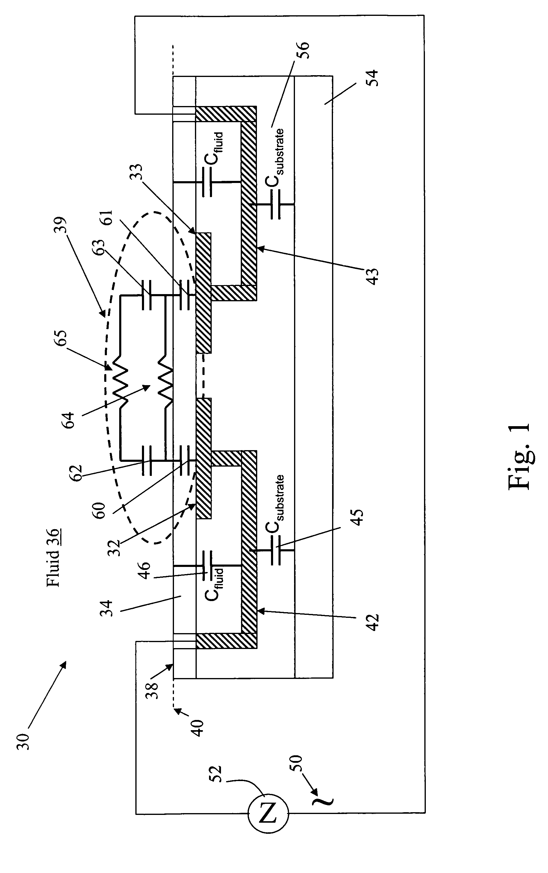
[0025]The present invention provides a surface micro sensor for monitoring the cleaning and drying processes on the surface of a dielectric film during the manufacture of ICs, MEMS and other micro devices. The surface of the dielectric can be non-porous, in which case the surface cleaning process is rate limited by the desorption of species from the surface or by removal of the species away from the surface. The dielectric can also be porous, or have other micro features present in it. Furthermore, a cell (biologic or other) may be placed on the surface and monitored.

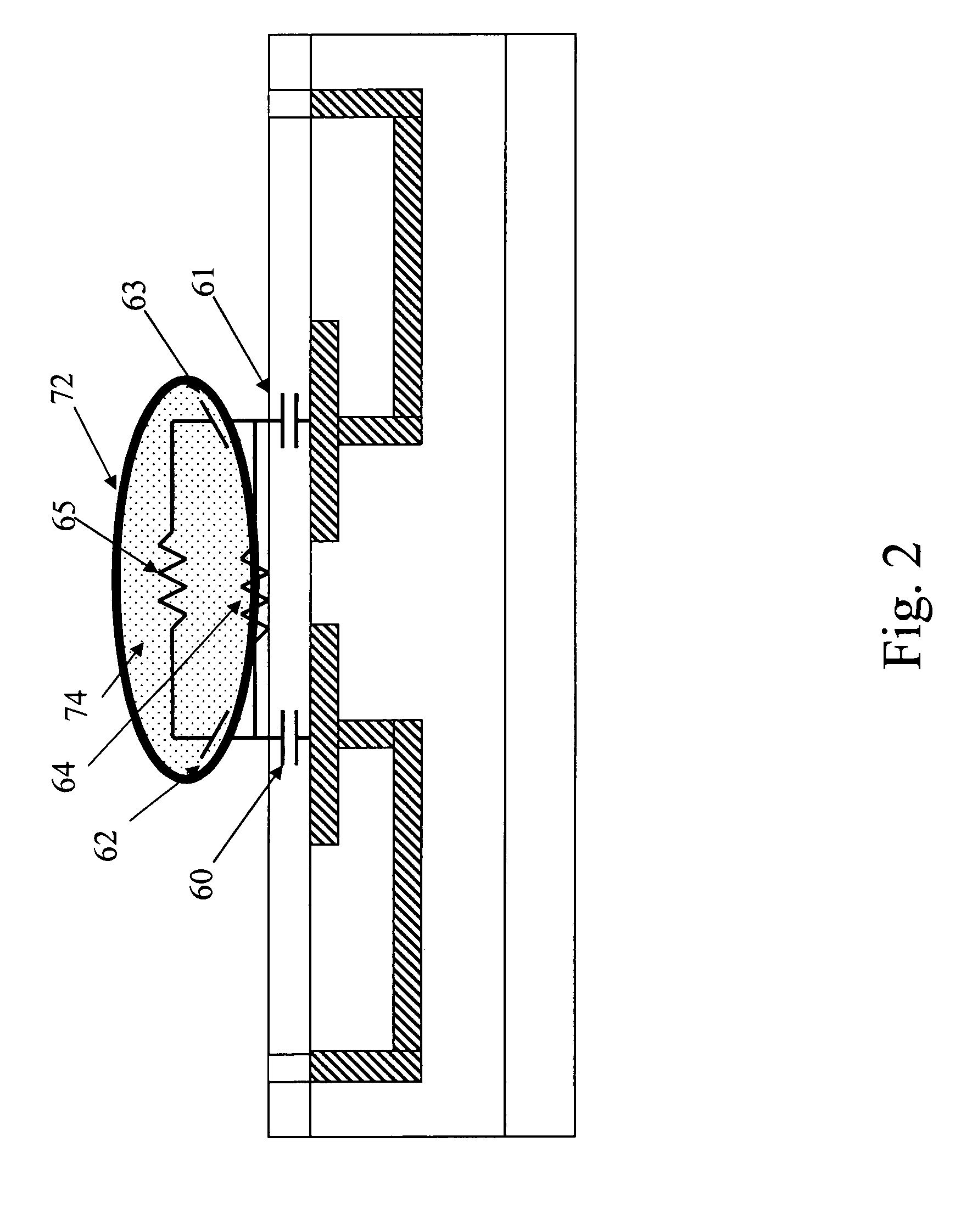
[0026]As shown in FIG. 1, an exemplary embodiment of a surface micro sensor 30 for in-situ monitoring of the process of cleaning, rinsing and drying of surfaces and the micro features in those surfaces comprises two conducting electrodes 32 and 33 (e.g. copper or doped polysilicon with a typical thickness of 1 μm) that lie in the same plane, embedded in the surface of a supporting dielectric 56 on a substrate 54 (e.g. a...


PUM


Abstract

The present invention provides a micro sensor for monitoring the cleaning and drying processes of surfaces of dielectric films, micro features in porous dielectric films and biologic or other cells common in microelectronics fabrication, MEMS fabrication or microbiology test system fabrication. By embedding electrodes in the surface of a supporting dielectric, the sensor can probe the surface and pores of a covering dielectric or a cell on the covering dielectric. The addition of a guard reduces the effects of any parasitic capacitance, which extends the measurement bandwidth of the sensor and allows it to be manufactured at the scale of a single cell, a feature that is particularly important for applications in microbiology.

Description

CROSS-REFERENCE TO RELATED APPLICATIONS[0001]This application claims benefit of priority under 35 U.S.C. 119(e) to U.S. Provisional Application No. 60 / 602,449 entitled “Electrochemical Residue Sensor for Porous Films” filed on Aug. 18, 2004 AND U.S. Provisional Application No. 60 / 624,131 entitled “Method For Impedance Monitoring Of Fluids And Gases In High Aspect Ratio Structures And Method For Manufacturing Such A Monitor” filed on Nov. 2, 2004, the entire contents of which are incorporated by reference.BACKGROUND OF THE INVENTION[0002]1. Field of the Invention[0003]This invention relates to monitoring the residue on a surface during a chemical treatment of the surface, such as cleaning and drying processes during the manufacture of ICs, MEMS and other micro devices and more specifically to a micro sensor for monitoring residue on and in dielectric films and cells on the surface of the sensor.[0004]2. Description of the Related Art[0005]A major challenge in manufacturing of the mic...

Claims


Application Information

Patent Timeline
IPC IPC(8): G01R27/00G01R27/04G01R27/08G01R27/32
CPCG01D5/24
Inventor VERMEIRE, BERT M.SHADMAN, FARHANG F.
Owner ENVIRONMENTAL METROLOGY CORP
Why Eureka
Try Eureka