Semiconductor memory

a semiconductor memory and memory cell technology, applied in the field of semiconductor memory, can solve the problems of large static noise margin in write operation, inability to achieve stable memory cell characteristics, etc., to achieve the effect of reducing the precharge level of bit lines, reducing the current injected to memory cells, and improving the write level

Active Publication Date: 2009-02-24
SOCIONEXT INC
View PDF5 Cites 25 Cited by
  • Summary
  • Abstract
  • Description
  • Claims
  • Application Information

AI Technical Summary

Benefits of technology

[0071]a potential of a high-data holding power supply coupled to the two inverter circuits is low when the temperature of the semiconductor memory is equal to or lower than a predetermined temperature which is within an operable-temperature range as compared with a case where the temperature of the semiconductor memory is higher than the predetermined temperature.
[0117]Further, the potential of the high-data holding power supply of the memory cell is low when the semiconductor memory operates at a voltage higher than a predetermined voltage which is within an operable-voltage range as compared with the case of a low supply voltage. With this measure, both the margins for reading and writing in the memory cell are secured, and the power consumed by the memory cell is decreased. Furthermore, the gate-source potential of a memory cell transistor is decreased to relax an electric field on an insulator film of the transistor, whereby the reliability of the semiconductor memory is improved.

Problems solved by technology

A disadvantage of these achievements is, for example, in the case of a semiconductor memory including flip flop type memory cells, such as a static random access memory (SRAM), a considerable difficulty in achieving stable memory cell characteristics due to variations in characteristics among transistors constituting memory cells or the decrease in supply voltage.
As a result of this disadvantage, the yield of such a semiconductor memory undesirably decreases due to static noise margin (SNM) or deterioration in write characteristics.
For example, when the write level is low, the margin for an erroneous writing due to bit line noise (static noise margin) becomes large in a write operation.
However, the time required for the write operation becomes long because the flip flop cannot be inverted before the potential of the bit line reaches a sufficiently low level.
On the other hand, when the write level is high, the margin for an erroneous writing (static noise margin) becomes small, although the time required for the write operation becomes short.
The write level being low means that the state of the flip flop of the memory cell unreadily inverts in the read operation due to bit line noise, or the like, i.e., that the static noise margin becomes large.
As described above, the write level and the static noise margin have conflicting characteristics with each other such that one of these characteristics cannot be satisfied without decreasing the other characteristic margin.
However, in a semiconductor memory in which the voltage of the high-data holding power supply of the memory cell is controlled as described above, the writing level is ameliorated but, when the high-data holding power supply of the memory cell is controlled to have a low voltage, the static noise margin is deteriorated.
However, when the potential of the word line is decreased, the write level deteriorates on the other hand.
Thus, even if the high-data holding supply voltage of the memory cell is decreased in a write operation such that the write level is ameliorated, the effect of such an arrangement is marred by a decrease in potential of the word line.
Therefore, the word line potential cannot be selectively high or low only at a crossing point of a selected column and a selected word line.
However, when a word line is selected for a write operation, the static noise margin undesirably deteriorates (writing occurs) in memory cells of unselected columns present on the same selected word line even though it is not intended.
In the case of a 2-port SRAM, the following problems arise in addition to the above-described disadvantages of the 1-port SRAM.
Therefore, the conventional technique of ameliorating only the read margin (static noise margin) or write margin (write level) by the control of the word line level in the word line direction or the control of the high-data holding power supply in the column direction cannot comply with such a semiconductor memory as a 2-port SRAM wherein write and read operations for memory cells on the same selected line are simultaneously carried out.

Method used


Image

  • Semiconductor memory
  • Semiconductor memory
  • Semiconductor memory

Examples


embodiment 1

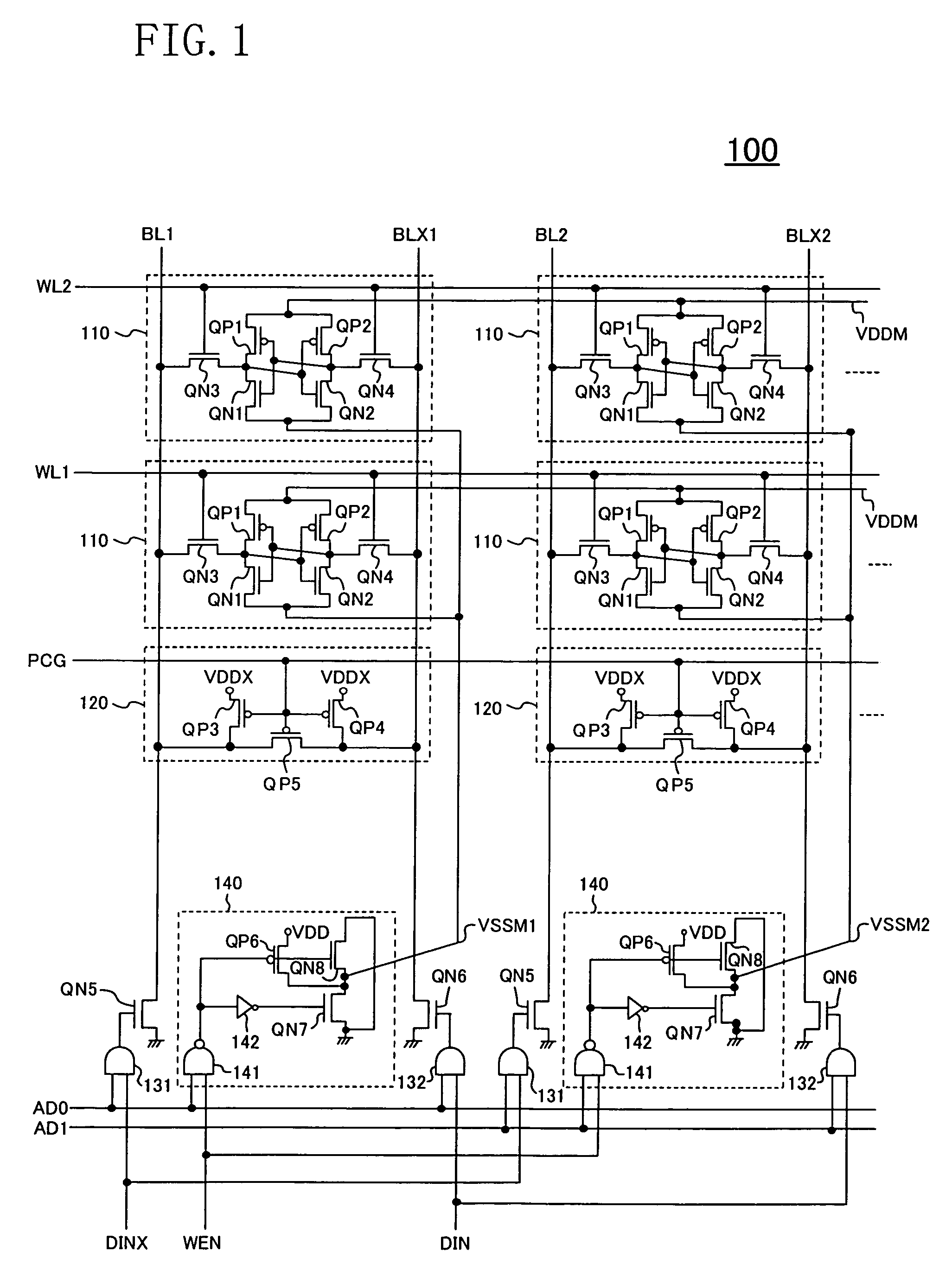
[0135]FIG. 1 is a block diagram showing the structure of a semiconductor memory 100 according to embodiment 1 of the present invention. It should be noted that, in FIG. 1, circuits for the reading system are omitted for simplicity of description.

[0136]Referring to FIG. 1, the semiconductor memory 100 includes memory cells 110, bit line precharge circuits 120, AND circuits 131 and 132, low-data holding power supply controlling circuits 140, and transistors QN5 and QN6 (N-type MOS transistors).

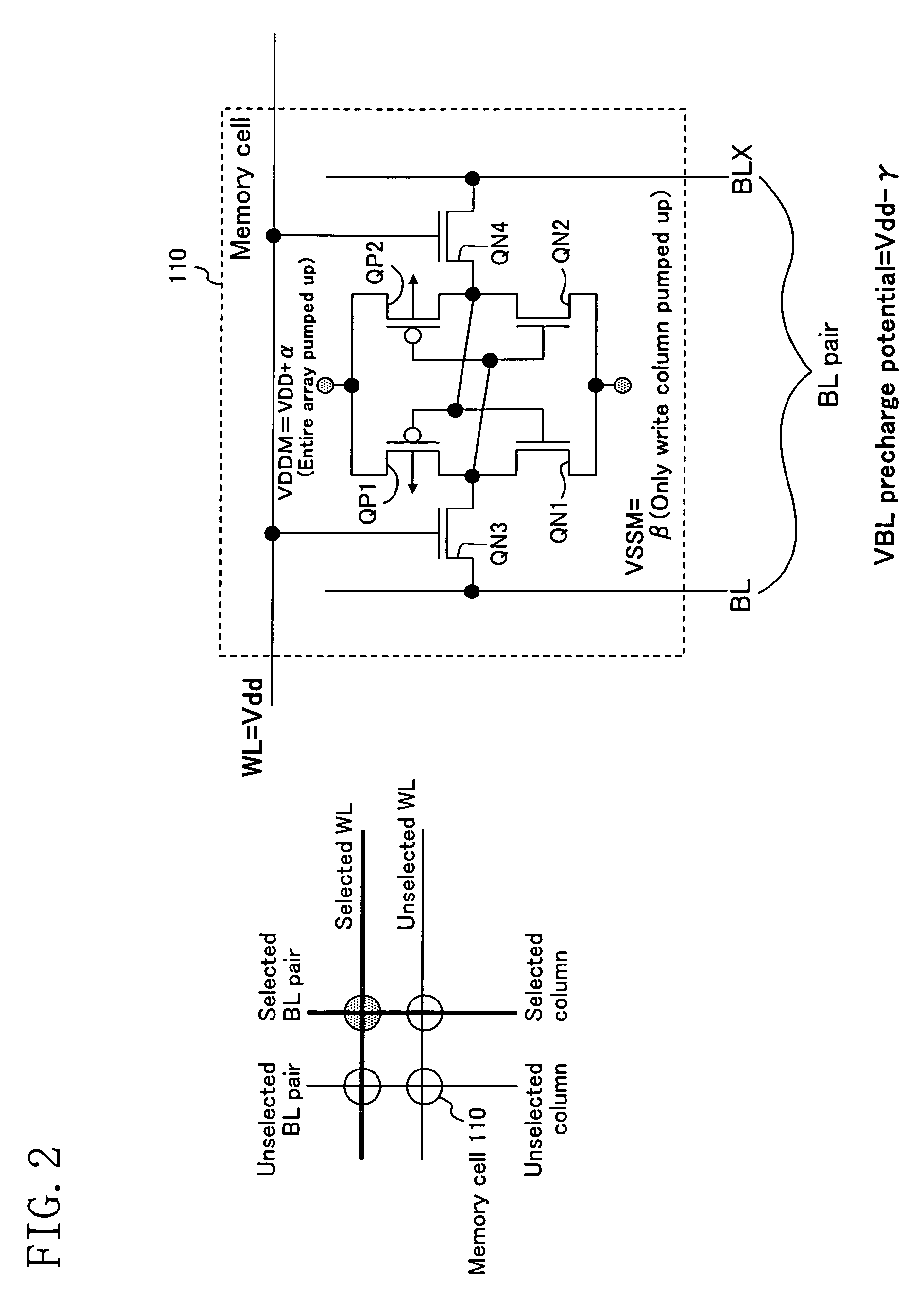
[0137]In FIG. 1, reference numerals WL1 and WL2 denote word lines. The word lines WL1 and WL2 extend in the row direction. The word lines WL1 and WL2 are connected to supply potential VDD when selected but connected to the ground when unselected.

[0138]Bit lines BL1, BL2, BLX1 and BLX2 extend in the column direction. Bit lines BL1 and BLX1 constitute a bit line pair, and bit lines BL2 and BLX2 constitute another bit line pair. One of each bit line pair (the pair of bit lines BL1 and BLX1 and the ...

embodiment 2

[0175]In embodiment 2, applications of the present invention to a 2-port SRAM which has two ports and a multi-port SRAM which has more than two access ports are described.

[0176]These semiconductor memories are also basically formed by cross-coupling of inverters for holding a pair of high data and low data. Therefore, the control technique of embodiment 1 for the memory cell low-data holding power supply, etc., can be commonly used in embodiment 2.

[0177]FIG. 4 is a block diagram showing the structure of a semiconductor memory 200 according to embodiment 2 of the present invention.

[0178]The semiconductor memory 200 includes memory cells 210 and low-data holding power supply controlling circuits 220 in place of the memory cells 110 and the low-data holding power supply controlling circuits 140 of the semiconductor memory 100. The semiconductor memory 200 further includes bit line precharge circuits 120, AND circuits 131 and 132, and transistors QN5 and QN6 as does the semiconductor me...

embodiment 3

[0193]FIG. 7 is a block diagram showing the structure of a semiconductor memory 300 according to embodiment 3 of the present invention. As shown in FIG. 7, the semiconductor memory 300 includes memory cells 310 in place of the memory cells 210 of the semiconductor memory 200 and further includes inverters 320.

[0194]Specifically, referring to FIG. 8, the memory cell 310 does not include the access transistor QN4 of the memory cell 210, and the write bit line is connected only to the access transistor QN3. That is, the number of write bit lines is smaller in the semiconductor memory 300 by one than in the semiconductor memory 200.

[0195]In FIG. 8, the current drivability of the access transistor QN3 is set larger than that of the drive transistors QN1 and QN2. For example, the current drivability may be set by setting the threshold value of the access transistor QN3 lower than that of the drive transistors QN1 and QN2. Alternatively, the setting may be realized by increasing the transi...


PUM


Abstract

In a semiconductor memory including word lines and bit lines arranged in a matrix and a plurality of memory cells provided at intersections of the word lines and the bit lines, a bit line precharge circuit is provided for controlling the potential of a low-data holding power supply coupled to memory cells provided on a corresponding one of the bit lines. In a write operation, the bit line precharge circuit controls the potential of a low-data holding power supply of a memory cell corresponding to a selected bit line to be higher than the potential of a low-data holding power supply of a memory cell corresponding to an unselected bit line.

Description

CROSS-REFERENCE TO RELATED APPLICATIONS[0001]This application claims priority under 35 U.S.C. §119(a) on Japanese Patent Application No. 2005-365102 filed on Dec. 19, 2005 and Japanese Patent Application No. 2006-151542 filed on May 31, 2006, the entire contents of the specification, drawings and claims of which are hereby incorporated by reference.BACKGROUND OF THE INVENTION[0002]1. Field of the Invention[0003]The present invention relates to a semiconductor memory including flip flop type memory cells and specifically to the technique of controlling the low-data holding power supply, high-data holding power supply, bit-line precharging power supply of the memory cells.[0004]2. Description of the Prior Art[0005]In recent years, along with the advancement of process miniaturization, the reduction in area of semiconductor integrated circuits and the decrease in supply voltage have been achieved on an accelerated basis. A disadvantage of these achievements is, for example, in the case...

Claims


Application Information

Patent Timeline
Patent Type & Authority Patents(United States)
IPC IPC(8): G11C11/00
CPCG11C5/14G11C11/412
Inventor SUZUKI, TOSHIKAZUYAMAGAMI, YOSHINOBUISHIKURA, SATOSHI
Owner SOCIONEXT INC
Why Eureka
Try Eureka