Semiconductor device and driving method of the same

a semiconductor device and semiconductor technology, applied in semiconductor devices, digital storage, instruments, etc., can solve the problems of insufficient security measures, inability to write data, and inability to meet the needs of users, so as to prevent rewriting, inexpensive semiconductor devices and a driving method of semiconductor devices, easy to deposit

Inactive Publication Date: 2009-03-03
SEMICON ENERGY LAB CO LTD
View PDF28 Cites 50 Cited by
  • Summary
  • Abstract
  • Description
  • Claims
  • Application Information

AI Technical Summary

Benefits of technology

[0008]It is an object of the present invention to provide a semiconductor device in which data can be written other than in manufacturing the semiconductor device and falsification by rewriting can be prevented. Further, it is an object of the present invention to an inexpensive semiconductor device that is easily formed and includes a memory element and a method for driving the semiconductor device.
[0023]In accordance with the present invention, it is possible to obtain a semiconductor device in which data can be written (write once read many) other than in manufacturing the semiconductor device and falsification by rewriting can be prevented. Further, it is possible to provide an inexpensive semiconductor device and a method for driving the semiconductor device by providing a memory using an organic compound that is easily deposited as a material or a semiconductor device including the memory.
[0024]Furthermore, it is possible to provide a semiconductor device including a memory element in which data can be written with small power.

Problems solved by technology

In this case, no writing of data can be carried out other than in manufacturing the chip, and the chip is thus not user-friendly.
Therefore, security measures are not implemented sufficiently now, and thus, measures that are able to prevent falsification by rewriting or the like have been needed.

Method used


Image

  • Semiconductor device and driving method of the same
  • Semiconductor device and driving method of the same
  • Semiconductor device and driving method of the same

Examples


embodiment mode 1

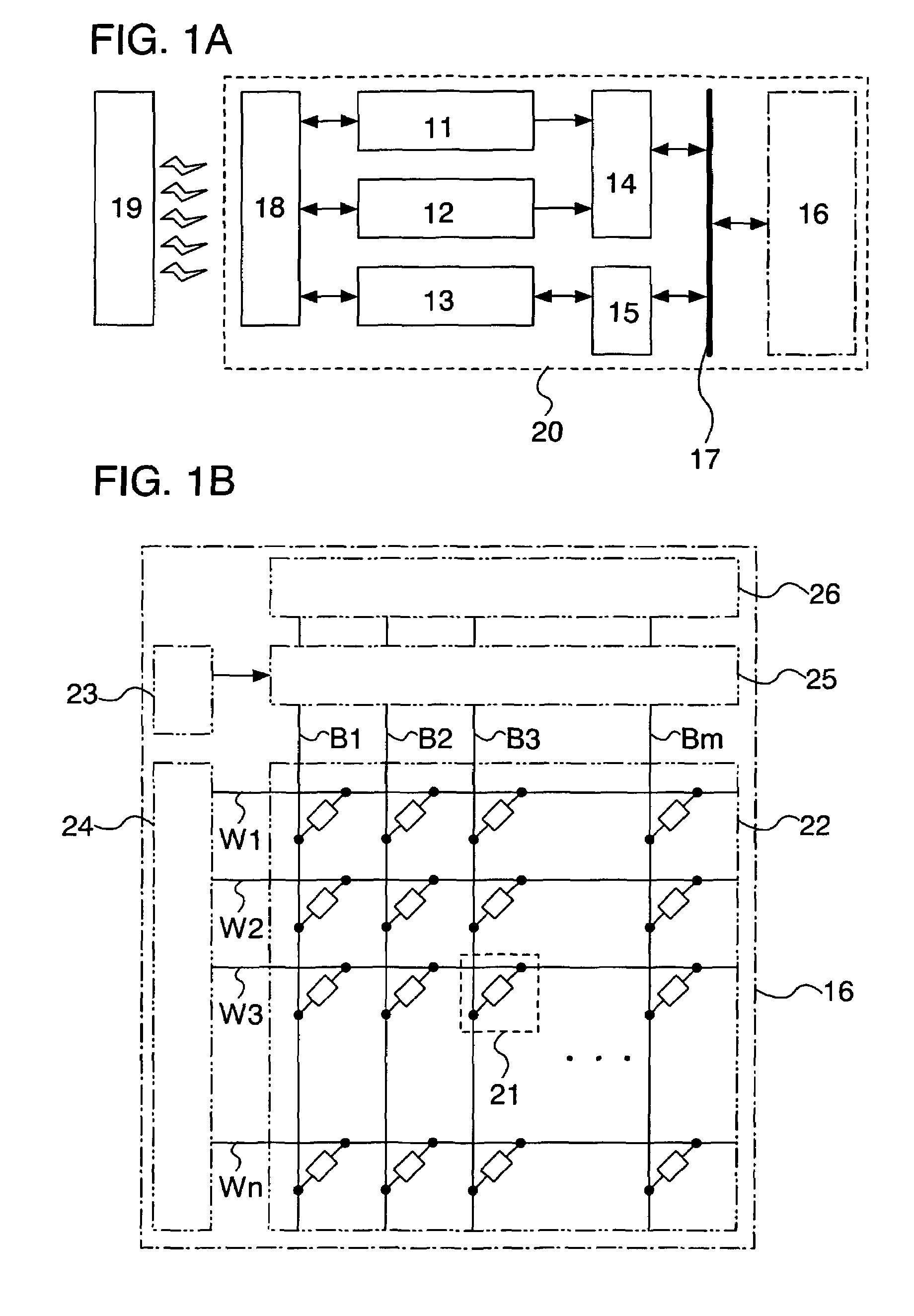
[0058]A semiconductor device 20 described in the present embodiment mode has a function of non-contact exchange of data, and includes a power supply circuit 11, a clock generation circuit 12, a data demodulation / modulation circuit 13, a control circuit 14 that controls other circuits, an interface circuit 15, a memory 16, a data bus 17, and an antenna 18 (an antenna coil) (FIG. 1A). The power supply circuit 11 is a circuit that generates various power sources to be supplied to each circuit in the semiconductor device 20, based on input an alternating-current signal from the antenna 18. The clock generation circuit 12 is a circuit that generates various clock signals to be supplied to each circuit in the semiconductor device 20, based on input an alternating-current signal from the antenna 18. The data demodulation / modulation circuit 13 has a function of demodulating / modulating data for exchange with a reader / writer 19. The control circuit 14 has a function of controlling the memory ...

embodiment mode 2

[0090]As described above, a semiconductor device has a memory. A semiconductor device that is different from the semiconductor device in the embodiment mode described above will be described below with reference to the accompanying drawings.

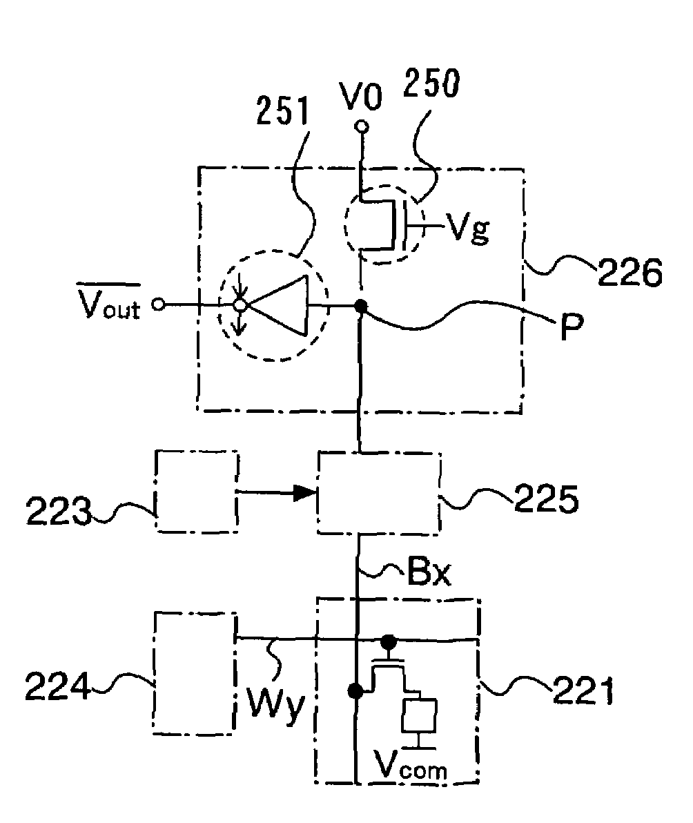
[0091]A memory 216 has a memory cell array 222 in which a memory cell 221 is provided in a matrix, decoders 223 and 224, a selector 225, and a read / write circuit 226 (FIG. 10). It is to be noted the structure of the memory 216 shown here is just an example, another circuit such as a sense amplifier, an output circuit, or a buffer may be included.

[0092]The memory cell 221 a first conductive layer connected to a bit line Bx (1≦x≦m), a second conductive layer connected to a word line Wy (1≦y≦n), a transistor 240, and a memory element 241 (hereinafter, also referred to as an organic memory element 241). The memory element 241 has a structure in which an organic compound layer is sandwiched between a pair of electrodes. The transistor 240 has a gate e...

embodiment mode 3

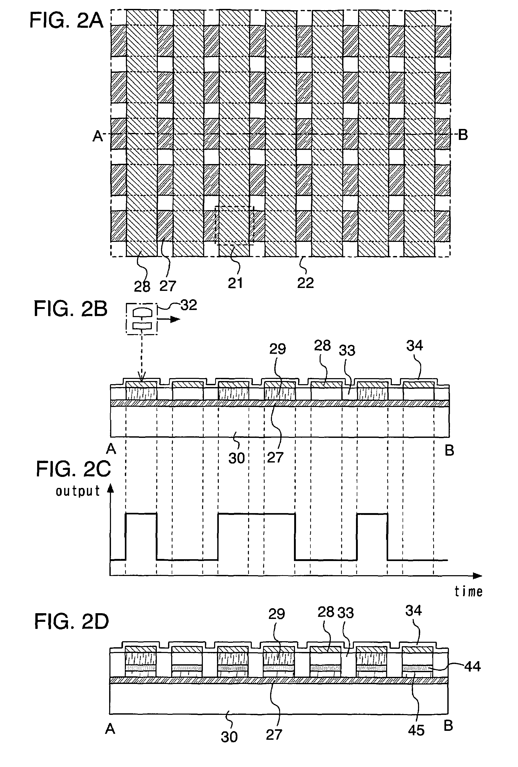
[0113]Writing of data in an organic memory included in a semiconductor device 20 according to the present invention is carried out by optical or electrical action. When writing of data is carried out by optical action, a plurality of semiconductor devices 20 are formed over a flexible substrate 31 and then irradiated with laser light by a laser light irradiating means 32 so that writing of data can be continuously carried out easily. Moreover, when this manufacturing process is employed, the semiconductor devices 20 can be easily manufactured in large quantity (FIG. 3A). Accordingly, the inexpensive semiconductor devices 20 can be provided.

[0114]In addition, an organic compound layer included in an organic memory element can be intentionally dissolved or destroyed by heating to the melting point or more. Namely, writing of data can be carried out also by heat treatment as long as different heating temperatures are used. Accordingly, a manufacturing process using different heating te...


PUM


Abstract

The present invention provides a semiconductor device including a memory that has a memory cell array including a plurality of memory cells, a control circuit that controls the memory, and an antenna, where the memory cell array has a plurality of bit lines extending in a first direction and a plurality of word lines extending in a second direction different from the first direction, and each of the plurality of memory cells has an organic compound layer provided between the bit line and the word line. Data is written by applying optical or electric action to the organic compound layer.

Description

TECHNICAL FIELD[0001]The present invention relates to a semiconductor device and a method for driving the semiconductor device.BACKGROUND ART[0002]In recent years, individual recognition technology has gotten a lot of attention. For example, there is a technology to be used for production and management, in which information such as a history of the object is clarified by giving an ID (an individual recognition number) to an individual object. Above all, the development of semiconductor devices that send and receive data without contact by using an electromagnetic field or a radio wave have been advanced. As such semiconductor devices, in particular, a wireless chip (also referred to as an ID tag, an IC tag, and IC chip, an RF (Radio Frequency) tag, a wireless tag, an electronic tag, or an RFID (Radio Frequency Identification)) is beginning to be introduced into companies, markets, and the like.[0003]Many of semiconductor devices that have been already been put to practical use have...

Claims


Application Information

Patent Timeline
Patent Type & Authority Patents(United States)
IPC IPC(8): G11C11/00
CPCB82Y10/00G11C13/0014G11C13/0059G11C16/22G11C17/16H01L27/285G11C13/04G11C2213/77G11C2213/79H01L51/0051H01L51/0059H10K19/202H10K85/611H10K85/631H10B63/80
Inventor NOMURA, RYOJIABE, HIROKOIWAKI, YUJIYAMAZAKI, SHUNPEI
Owner SEMICON ENERGY LAB CO LTD
Why Eureka
Try Eureka