Over-voltage tolerant pass-gate

a technology of mosfet transistor and pass-gate, which is applied in the direction of pulse generator, pulse technique, instruments, etc., can solve the problems of trouble, low power supply level, and threshold requirements inherent in mosfet transistors, so as to reduce leakage, reduce gate leakage, and reduce the effect of large well leakag

Active Publication Date: 2009-04-07
SEMICON COMPONENTS IND LLC
View PDF14 Cites 19 Cited by
  • Summary
  • Abstract
  • Description
  • Claims
  • Application Information

AI Technical Summary

Benefits of technology

[0016]The present invention provides for the well or wells of the primary switch FETs to be driven so that the inherent pn junctions and the parasitic transistors do not become forward biased by the various power supply voltage and signal level voltages that may be found in pass-gate operations. That is, a +1.8 voltage signal being transferred via electronics powered from +5V to another +5V logic system will not suffer high leakage, breakdowns or other malfunctions.
[0020]The present invention provides a mechanism to reduce leakage at the wells and the gates of the primary switches, and to ensure proper enablement of the switches under the various signal and power levels encountered by a pass-gate. In this regard the power supply for the circuit that is meant to turn on and off the pass-gate (the enabling circuit) has a circuit, in one embodiment, that is identical to that connected to the well of a PMOS primary switch transistor. The separate circuit used to drive the enabling circuit, even though it may be identical to the circuit connected to the well of the PMOS primary switch, has the beneficial effect of reducing any gate leakage without negatively affecting the reduction of larger well leakage.

Problems solved by technology

Operation at the lower power supply levels, however, encounters issues with respect to threshold requirements inherent in MOSFET transistors.
For example, in systems with differing power sources, trouble might be encountered where a logic signal sent from a system is higher than the power supply of the receiving system.
Over / under-voltage effects are known to cause catastrophic MOSFET failures.
Other approaches, as in the above referenced patent application, may not provide full over / under-voltage protection during power up and / or power down operations.
The '099 low insertion loss circuit embodiment, however, may have larger leakage when there is a signal voltage present and the supply voltage to the transfer switch is turned off, e.g., when power is turned off first to the transfer switch before it is turned off at the sending or receiving systems.
However, if the +V supply is at ground (by the supply being turned off) while there is a high logic level, say +5V, at terminal A, the pn drain-well diode in the MOSFET switch is forward biased creating a potentially harmful current path that charges the output capacitor of the +V supply.
Well current to the Vdd power supply rail may be termed well leakage and remains an issue in some prior art circuits.
One bias condition exists where the potential differences among the drain, source and Vdd may be too small for known circuitry to correctly resolve.
There remain, in prior art MOSFET pass-gate switches, limitations in providing over-voltage tolerance and protection for all values of supply power (Vdd) as may be encountered during normal operations and / or during power up and power down operations.
Prior art circuits are especially vulnerable during power up operations, where, for example, an off pass-gate may not remain off during such operations and where excessive leakage currents may occur.

Method used


Image

  • Over-voltage tolerant pass-gate
  • Over-voltage tolerant pass-gate
  • Over-voltage tolerant pass-gate

Examples


Embodiment Construction

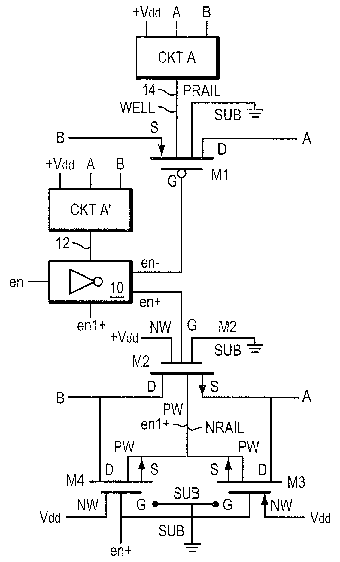
[0030]FIG. 1 has a PMOS, M1, and an NMOS, M2, in parallel, joining point A to point B. These two MOS transistors are the primary parallel transistor switches that comprise a pass-gate. The substrate contacts, SUB, of each of the transistor switches are functionally connected to ground. The WELL of PMOS M1 is tied to CKT A, its gate G to an enable signal, en−, its drain to external contact A and its source to external contact B. In normal operation the pass-gate transfers signals from A to B or vice versa.

[0031]The drain of the parallel NMOS, M2, is functionally connected to external contact B, and its source to external contact A. As known to those skilled in the art, the drain and source of these transistors often may be reversed with no effect. The gate G of M2 is connected to a positive true enable signal, en+, and to the gates of M2 and M3, as discussed below. The PW (P Well) is connected to a positive true enable signal, en1+, and the NW (N-Well) of the M2 is connected to +Vdd....


PUM


Abstract

A pass-gate having a single or parallel opposite polarity FETs is disclosed. The wells of the primary transistor switches are driven from circuitry that reduces over-voltage leakage and other malfunctions. A circuit that drives the wells is also used to power enable circuits that drive the gates of the pass transistors. The use of separate circuits to the gate and the wells further reduces leakage. In the condition of power supply voltage and signal levels that are near the thresholds of the FETs involved, one or more Schottky diodes may be used across pn junctions in the FETs that will prevent turning on the pn junctions.

Description

CROSS-REFERENCE TO RELATED APPLICATIONS[0001]The present application is related to an application, owned by the same entity, entitled, Method for Reducing Insertion Loss and Providing Power Down Protection in MOSFET Switches, Ser. No. 11 / 673,259, which was filed on Aug. 18, 2004. This prior application is hereby incorporated herein by reference.BACKGROUND OF THE INVENTION[0002]1. Field of the Invention[0003]The present invention relates to MOSFET devices and particularly to MOSFET devices used as low on-impedance switches.[0004]2. Background Information[0005]MOSFET switches are found in many applications and have become common in high frequency, pass-gate switch applications. As technology progressed, such transistor switches became smaller, faster and more power efficient. Often these low on-impedance switches are used to transfer logic data between systems using different power sources, say a 5V system sending and / or receiving logic signals from a 3V system. Typically the power so...

Claims


Application Information

Patent Timeline
Patent Type & Authority Patents(United States)
IPC IPC(8): H03K3/01
CPCH03K17/08142H01L29/1087H03K17/6874H03K17/693H03K17/6871H01L29/78H03K17/302H03K2217/0018H03K17/16H03K17/687
Inventor MISKE, MYRON J.
Owner SEMICON COMPONENTS IND LLC
Why Eureka
Try Eureka