Method of manufacturing semiconductor device and semiconductor device formed by the method

a manufacturing method and semiconductor technology, applied in the direction of semiconductor devices, basic electric elements, electrical apparatus, etc., can solve the problems of insufficient activation of impurity ions, inability to use inexpensive fz wafers, and inability to activate insufficiently implanted impurity ions, etc., to facilitate manufacturing a semiconductor device, reduce manufacturing costs, and reduce manufacturing costs

Active Publication Date: 2009-04-14
FUJI ELECTRIC CO LTD
View PDF22 Cites 4 Cited by
  • Summary
  • Abstract
  • Description
  • Claims
  • Application Information

AI Technical Summary

Benefits of technology

[0012]Although crystal defects are introduced into the first semiconductor layer by the charged particle beam irradiation, the region from the exposed surface exposed by grinding, that is the laser-irradiated surface, to a predetermined depth is recovered from the defective state caused by the crystal defects introduced therein. Since the minority carrier lifetime in the recovered region from the laser-irradiated surface to the predetermined depth is restored to the value before the charged particle beam irradiation, the soft recovery characteristics can be improved.
[0013]The charged particle beam can be irradiated after forming the second semiconductor layer and the first electrode on the first major surface of the first semiconductor layer. Since the impurity activation and crystal defects removal are conducted based on the local heating by laser beam irradiation, the second semiconductor layer doped with a predetermined concentration of impurity and the first electrode, both formed before the laser beam irradiation on the first major surface of the first semiconductor layer opposite to the second major surface irradiated with the laser beams, are not affected. Therefore, any device structure formed on the first major surface of the first semiconductor layer does not pose any problem on introducing crystal defects into the first semiconductor layer and recovering the region in the second surface portion of the first semiconductor layer from the defective state.
[0018]The charged electron beam can be an electron beam. By using an electron beam, crystal defects are introduced uniformly into the semiconductor substrate. The first semiconductor layer or substrate can be formed from an FZ wafer. Since the FZ wafer is less expensive than the epitaxial wafer, the semiconductor device can be obtained with lower manufacturing costs.
[0019]The manufacturing method according to the invention that includes the step of grinding the back surface of a semiconductor substrate facilitates manufacturing a semiconductor device that exhibits soft recovery characteristics. In particular, a diode having decreased reverse recovery time and reverse recovery losses thereof and improved soft recovery characteristics thereof can be obtained. Moreover, IGBT modules and intelligent power modules (hereinafter referred to as “IPMs”), which cause low electrical losses and low radiative electromagnetic noises and consider the environmental problems, can be formed.

Problems solved by technology

Due to the activation at a lower temperature, the implanted impurity ions are liable to be activated insufficiently.
The method disclosed in the Japanese published application above that uses an epitaxial wafer, however, is not suitable for using the inexpensive FZ wafer, which has been used mainly in these days.

Method used


Image

  • Method of manufacturing semiconductor device and semiconductor device formed by the method
  • Method of manufacturing semiconductor device and semiconductor device formed by the method
  • Method of manufacturing semiconductor device and semiconductor device formed by the method

Examples


Embodiment Construction

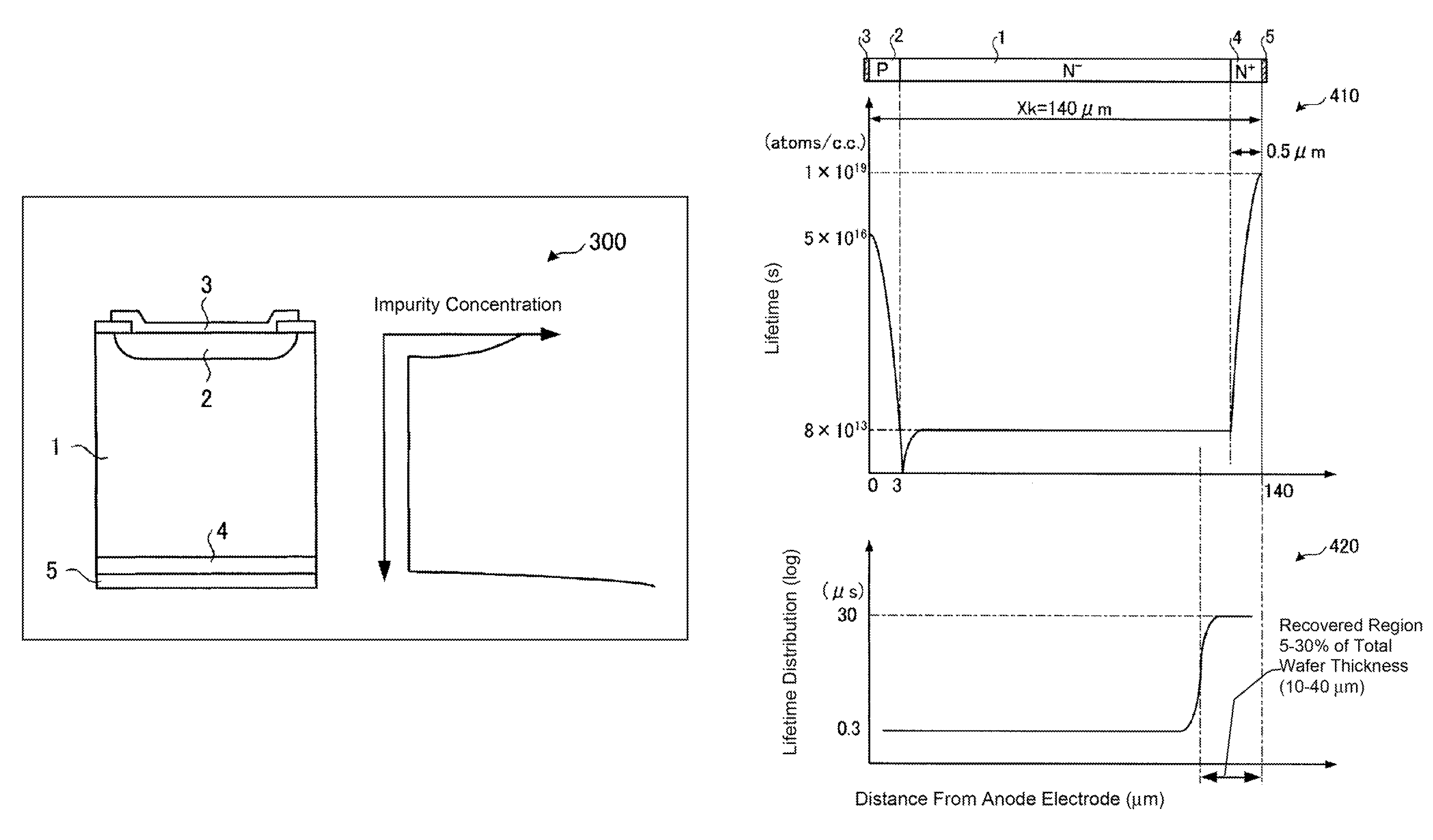
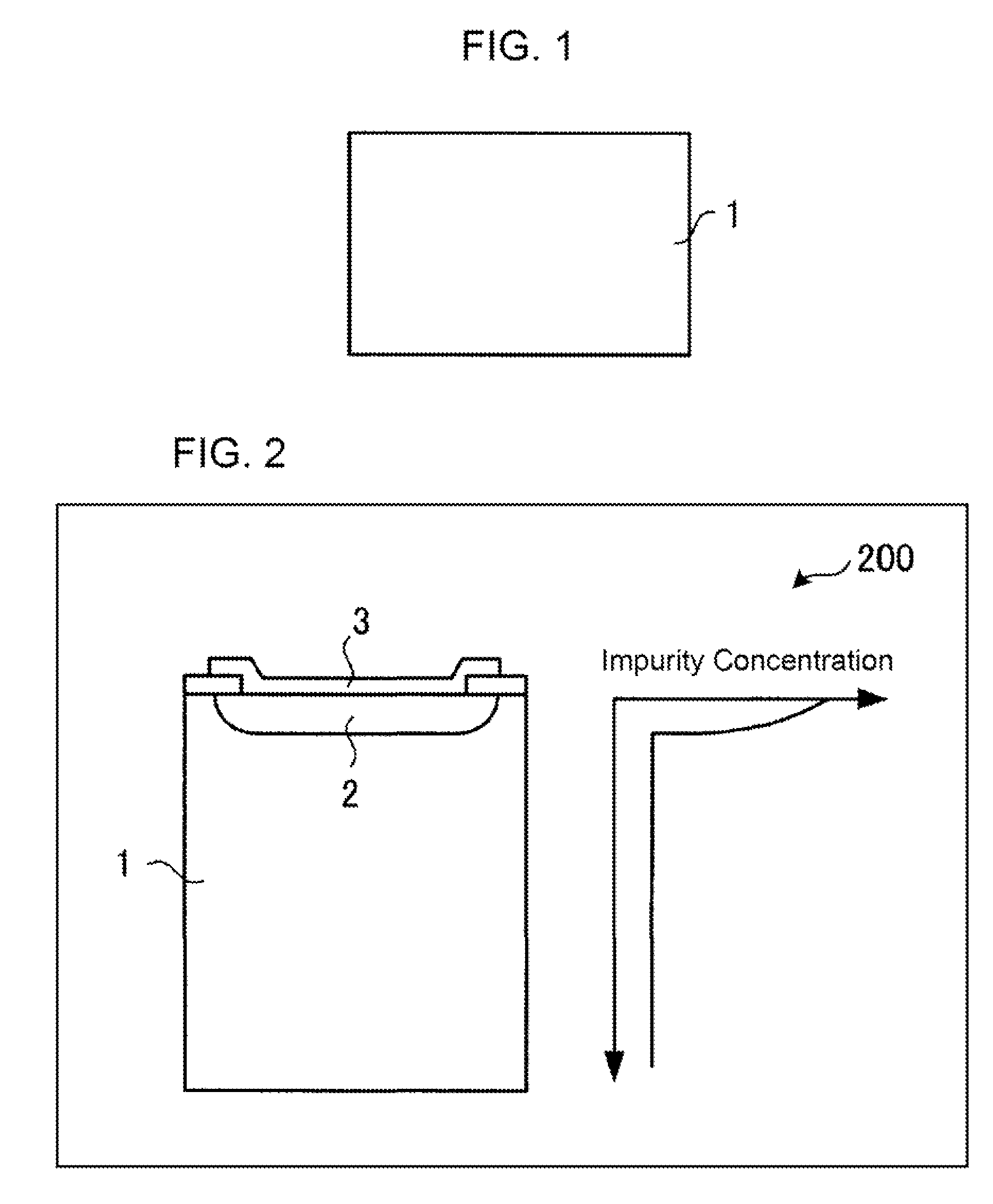
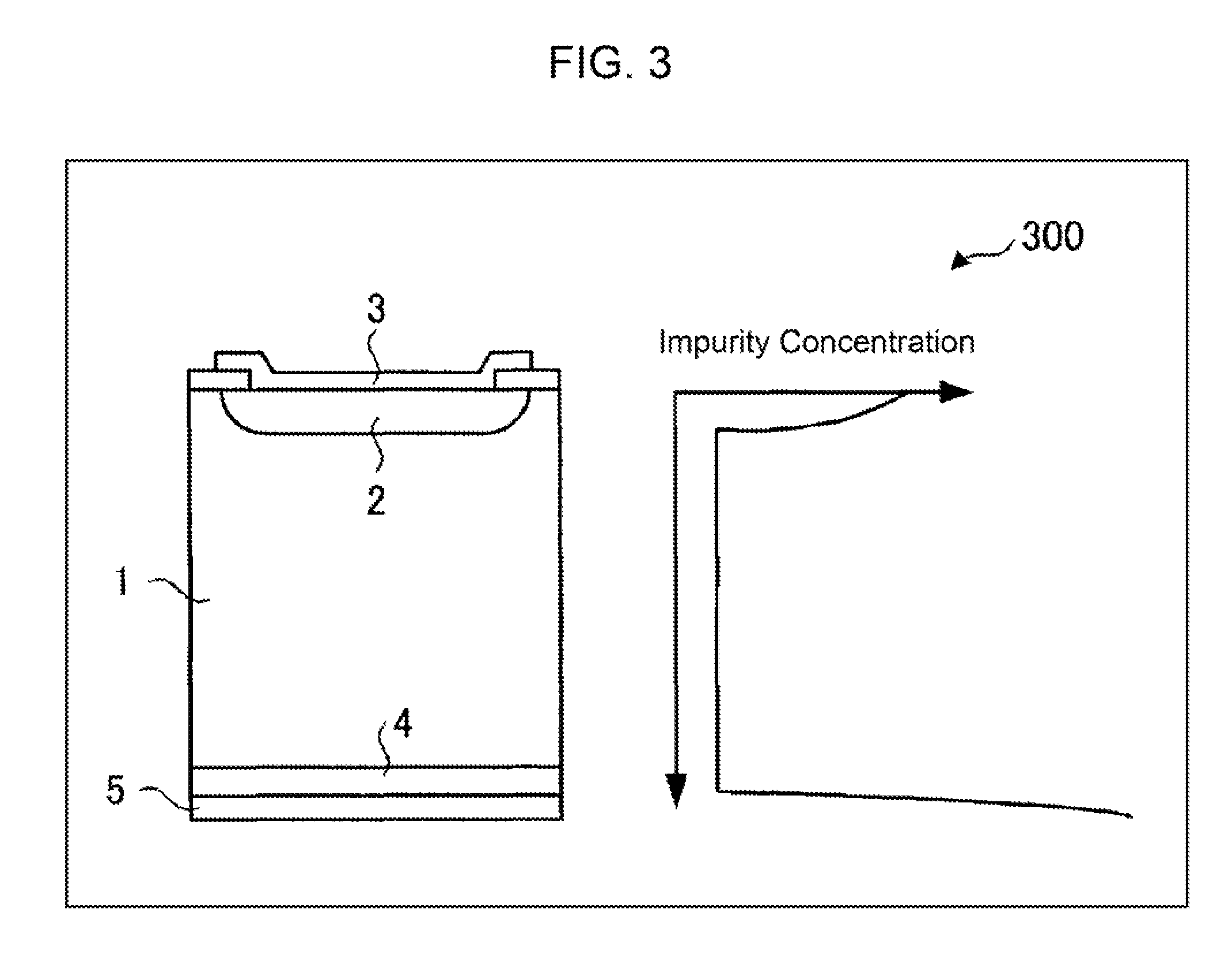
[0034]The present invention will be described in detail hereinafter with reference to the accompanied drawings, which illustrate the specific exemplary embodiments according to the present invention. In the following descriptions, the n-type layer or the n-type region is a layer or a region where the electrons are majority carriers. The p-type layer or the p-type region is a layer or a region where the holes are majority carriers. The superscript “+” following the letter “n” or “p” indicating the conductivity type of the layer or the region indicates that the layer or the region is doped relatively heavily. The superscript “−” following the letter “n” or “p” indicating the conductivity type of the layer or the region indicates that the layer or the region is doped relatively lightly. Throughout the following descriptions and the attached drawings, the same reference numerals are used to designate the same or like constituent elements and their duplicated explanations are omitted for...


PUM


Abstract

The method of manufacturing a semiconductor device includes forming a p-type anode layer and an anode electrode on one major surface of an n-type semiconductor substrate, irradiating an electron beam to the semiconductor substrate to introduce crystal defects into the semiconductor substrate, grinding the other major surface of semiconductor substrate to reduce the thickness the semiconductor substrate, implanting phosphorus ions from the exposed surface of semiconductor substrate, and irradiating pulsed YAG laser beams by the double pulse technique to the exposed surface, from which the phosphorus ions have been implanted, to activate the implanted phosphorus atoms and to recover the region extending from the exposed surface irradiated with the YAG laser beams to the depth corresponding to 5 to 30% of the total wafer thickness from the defective state caused by the crystal defects introduced therein.

Description

BACKGROUND[0001]The known conventional method of manufacturing diodes, insulated gate bipolar transistors (hereinafter referred to as “IGBTs”) and such power semiconductor devices uses a thick silicon wafer. At the final stage of the manufacturing process, the thick silicon wafer is ground thin and thereafter etched to form a predetermined final thickness. Thereafter, implanted ions are activated by an activation heat treatment. See for instance, published PCT application WO 00 / 04596 or. Japanese published patent application 2002-520885. Recently, the manufacturing process described above has been mainly employed.[0002]Since electrodes have been formed already on the semiconductor wafer surface opposite to the surface thereof ground thin, it is necessary to conduct the activation heat treatment below the melting point of the electrode material, e.g., below 450° C. for aluminum. Due to the activation at a lower temperature, the implanted impurity ions are liable to be activated insuf...

Claims


Application Information

Patent Timeline
Patent Type & Authority Patents(United States)
IPC IPC(8): H01L21/425
CPCH01L21/26513H01L21/268H01L29/66128H01L29/8611H01L21/263
Inventor NEMOTO, MICHIOKIRISAWA, MITSUAKINAKAZAWA, HARUO
Owner FUJI ELECTRIC CO LTD
Why Eureka
Try Eureka