Semiconductor laser and method of fabricating the same

a semiconductor laser and laser technology, applied in semiconductor lasers, active medium materials, nanoinformatics, etc., can solve the problems of surface non-radiative recombination, difficult to ensure high-speed modulation operation, etc., and achieve the effect of high-speed modulation operation

Active Publication Date: 2009-04-21
FUJITSU LTD +1
View PDF19 Cites 29 Cited by
  • Summary
  • Abstract
  • Description
  • Claims
  • Application Information

AI Technical Summary

Benefits of technology

[0013]It is therefore an object of the present invention to provide a semiconductor laser capable of ensuring high-speed modulation operation and a high level of reliability, even if a p-type doped quantum dot active layer is used, and a method of fabricating the same.

Problems solved by technology

The present inventors made extensive investigations aiming to clarify causes for the above-described problems, and found out that the conventional ridge-structured semiconductor laser had a large parasitic capacitance ascribable to a large area of the p-n junction plane, and this made it difficult to ensure high-speed modulation operation.
Formation of the high mesa structure, however, needs etching of the individual layers composing the quantum dot active layer 103, and this undesirably induces the surface non-radiative recombination and the like.

Method used


Image

  • Semiconductor laser and method of fabricating the same
  • Semiconductor laser and method of fabricating the same
  • Semiconductor laser and method of fabricating the same

Examples


first embodiment

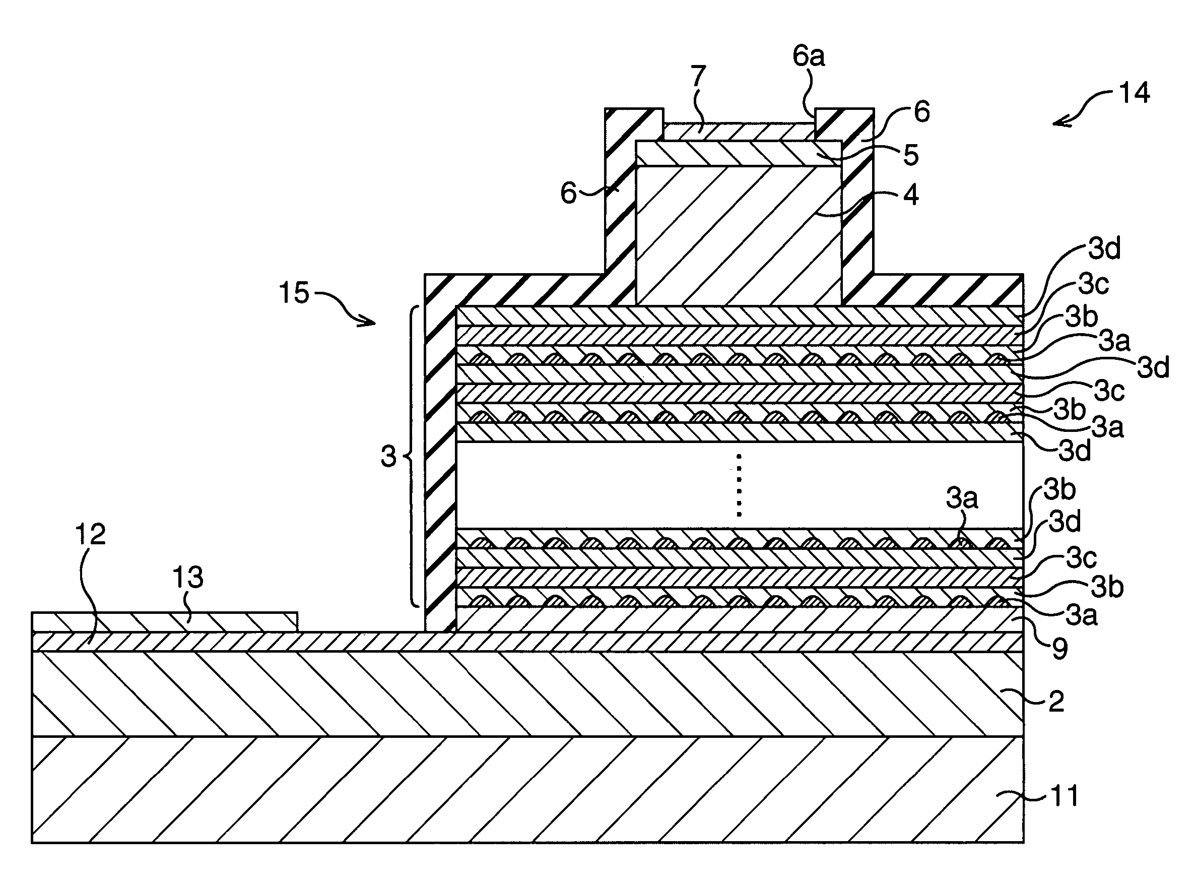
[0025]The first embodiment of the present invention will be described. It is to be noted that a structure of the semiconductor laser will be described in conjunction with a method of fabrication of the same for the convenience's sake. FIGS. 1A to 1E are sectional views sequentially showing a method of fabricating the semiconductor laser according to the first embodiment of the present invention.

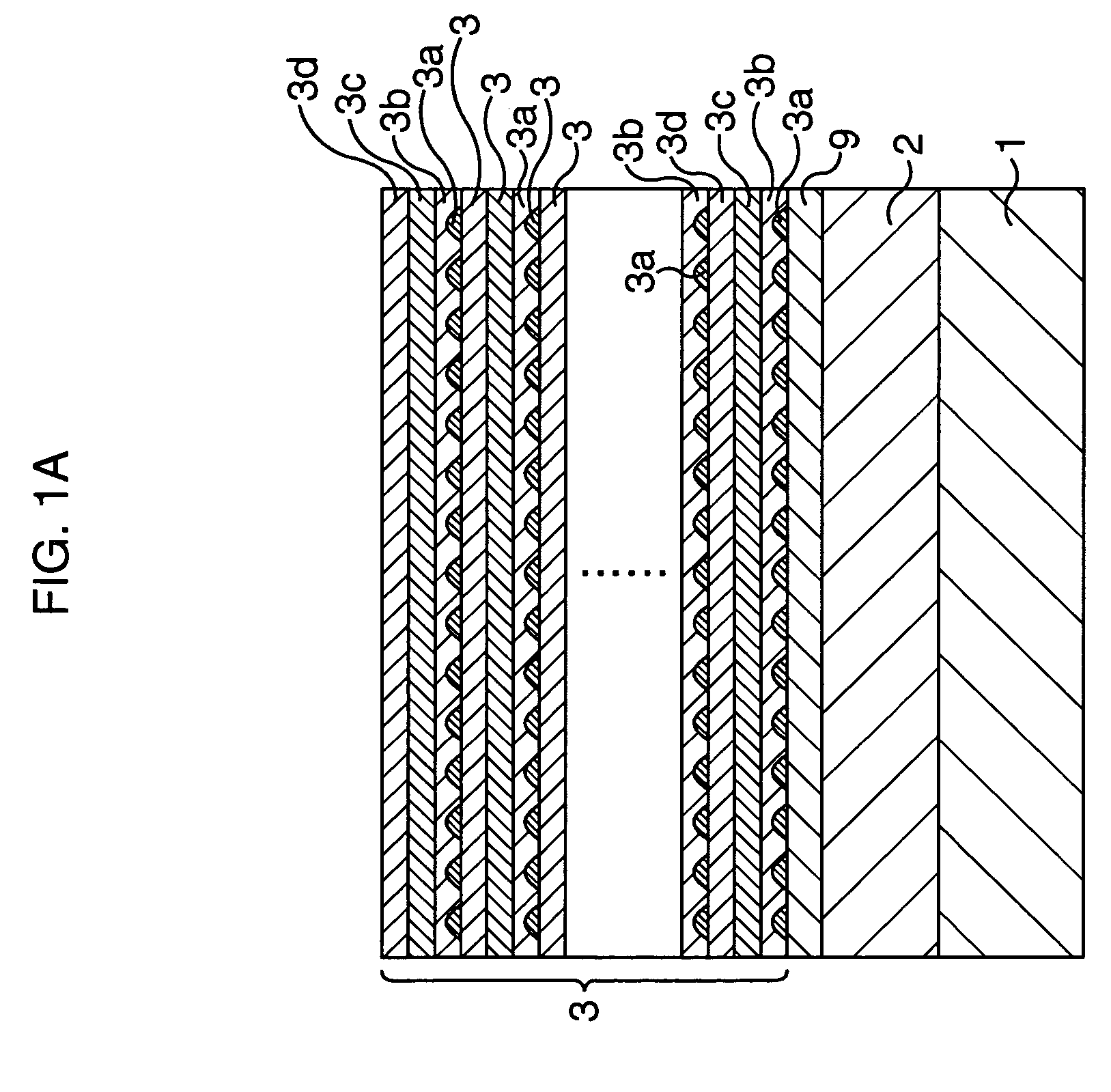
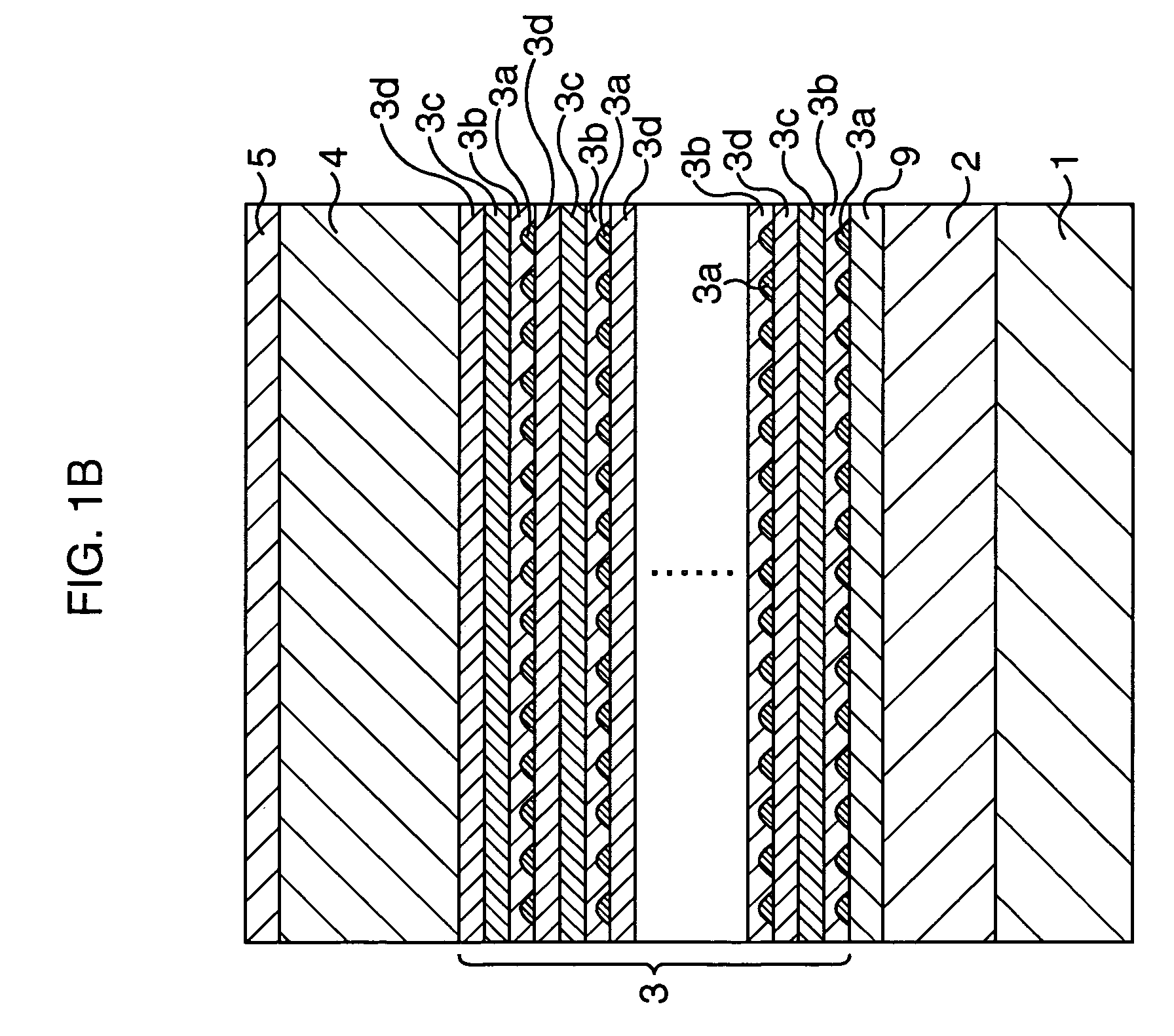
[0026]In this embodiment, first, as shown in FIG. 1A, a p-type Al0.4Ga0.6As cladding layer 2 and a non-doped intrinsic GaAs waveguide layer 9 are formed in this order on a p-type GaAs substrate 1. The p-type GaAs substrate 1 used herein is such as having a (001) surface, for example. The thicknesses of the p-type Al0.4Ga0.6As cladding layer 2 and the intrinsic GaAs waveguide layer 9 are set to 1.4 μm or around, and 36 nm or around, respectively.

[0027]Next, a p-type quantum dot active layer 3 is formed on the intrinsic GaAs waveguide layer 9. Formation of the p-type quantum dot active layer 3 ...

second embodiment

[0037]Next, paragraphs will explain the second embodiment of the present invention. The description here will be made mainly on aspects different from those in the first embodiment. FIG. 2 is a sectional view showing a semiconductor laser according to the second embodiment of the present invention.

[0038]In the second embodiment, first, as shown in FIG. 2, the p-type Al0.4Ga0.6As cladding layer 2 and a p-type GaAs contact layer 12 are formed in this order on a n-type GaAs substrate 11. The n-type GaAs substrate 11 used herein is such as having a (001) surface. It is also allowable to use a high-resistivity GaAs substrate, in place of the n-type GaAs substrate 11. The thickness of the p-type GaAs contact layer 12 is 0.4 μm, for example.

[0039]Next, similarly to as described in the first embodiment, the intrinsic GaAs waveguide layer 9, the quantum dot active layer 3, the n-type Al0.4Ga0.6As cladding layer 4 and the n-type GaAs contact layer 5 are formed in this order on the p-type GaAs...

third embodiment

[0042]Next paragraphs will describe the third embodiment of the present invention. FIG. 3 is a sectional view showing a semiconductor laser according to the third embodiment of the present invention.

[0043]In the third embodiment, an n-type Al0.4Ga0.6As cladding layer 4a is formed on the quantum dot active layer 3. The thickness of the n-type Al0.4Ga0.6As cladding layer 4a is set to 150 nm, for example. An n-type AlAs layer 21 is formed on the center portion of the n-type Al0.4Ga0.6As cladding layer 4a, and an AlAs oxide layer 22 is formed around the n-type AlAs layer 21. The thickness of the n-type AlAs layer 21 and the AlAs oxide layer 22 is 30 nm, for example. An n-type Al0.4Ga0.6As cladding layer 4b is formed on the n-type AlAs layer 21 and the AlAs oxide layer 22. The thickness of the n-type Al0.4Ga0.6As cladding layer 4b is 1.25 μm or around, for example. Other configurations are same as those in the first embodiment.

[0044]In thus-configured third embodiment, the n-type AlAs la...


PUM


Abstract

An intrinsic GaAs waveguide layer is formed on a p-type AlGaAs cladding layer, a quantum dot active layer is formed further thereon. An n-type AlGaAs cladding layer is formed on the center portion of the quantum dot active layer. Thus-configured semiconductor laser is allowed to successfully suppress the area of the p-n junction plane to a small level, and to obtain a high level of reliability, because there is no need of processing the center portion of the quantum dot active layer, contributive to laser oscillation.

Description

CROSS-REFERENCE TO RELATED APPLICATIONS[0001]This application is based upon and claims the benefit of priority from the prior Japanese Patent Application No. 2005-104448, filed on Mar. 31, 2005, the entire contents of which are incorporated herein by reference.BACKGROUND OF THE INVENTION[0002]1. Field of the Invention[0003]The present invention relates to a semiconductor laser suitable for a light source in optical fiber communication, and a method of fabricating the same.[0004]2. Description of the Related Art[0005]Conventionally-used semiconductor lasers are such as those having a non-doped quantum dot active layer formed on an n-type substrate. In recent years, investigation into semiconductor lasers having formed therein a p-type-doped or p-type-modulation-doped (the both will generally be referred to as “p-type-doped”, hereinafter) quantum dot active layer, in place of the non-doped quantum dot active layer. The latter semiconductor laser is increased in the differential gain a...

Claims


Application Information

Patent Timeline
Patent Type & Authority Patents(United States)
IPC IPC(8): H01S5/00
CPCB82Y10/00B82Y20/00H01S5/341H01S5/0206H01S5/0422H01S5/06226H01S5/22H01S5/3054H01S5/3086H01S5/309H01S5/3412H01S5/34306
Inventor HATORI, NOBUAKIYAMAMOTO, TSUYOSHIOTSUBO, KOJIARAKAWA, YASUHIKO
Owner FUJITSU LTD
Why Eureka
Try Eureka