Semiconductor device, power converter device using it, and hybrid vehicle using the power converter device

a technology of power converter and semiconductor element, which is applied in the direction of semiconductor device, semiconductor/solid-state device details, electrical apparatus, etc., can solve the problems of prior art having reliability problems, contact portions being weaker against stresses, and limiting the application of objects, so as to improve the long-term reliability of contact portions, and improve the heat releasability

Inactive Publication Date: 2009-05-05
HITACHI LTD
View PDF12 Cites 15 Cited by
  • Summary
  • Abstract
  • Description
  • Claims
  • Application Information

AI Technical Summary

Benefits of technology

[0014]It is an object of this invention to provide a power semiconductor device capable of retaining its long-term reliability even in high temperature environments.
[0019]In accordance with the invention, it is possible to improve the long-term reliability of contact portions of semiconductor elements with respect to high temperature environments.
[0020]In addition, according to the invention, it is possible to improve heat release / radiation capabilities of the semiconductor elements. While in the semiconductor device a power semiconductor element for performing current switching operations is the component that becomes the highest temperature, it is possible for the invention to lower, by the improvement of the heat releasability, a temperature of more than one contact portion between a hybrid wiring board and the power semiconductor element, when compared to a case where prior known wires are directly connected to the power semiconductor element.
[0021]The temperature decrease of the contact portion means reduction of thermal expansion at such portion. Thus, according to the invention, it is possible to improve the long-term reliability in comparison with the case where wires are in direct contact with the power semiconductor element.
[0022]Additionally, the semiconductor device of this invention may be applied to a power conversion device for use in hybrid vehicles. At this time, the power converter is mountable at locations of high temperature environments. This makes it possible to provide a power converter device capable of acquiring long-term reliability without having any dedicated cooling machine.

Problems solved by technology

Thus, problems have arisen as to a limit to applicable objects.
Thus, when applied thereto, the prior art must be faced with reliability problems for the reasons presented below.
First, in the case of the prior art, when exposed to high temperatures, the temperature of a semiconductor element rises up to the glass-transition temperature of a conductive resin material or therearound.
This temperature riseup causes the resin material to become softer, resulting in contact portions being weaker against stresses.
However, this is difficult because the conductive resin material is inherently large in electrical resistance.
Accordingly, it remains difficult to reduce the amount of heat generation due to electrical conduction.

Method used


Image

  • Semiconductor device, power converter device using it, and hybrid vehicle using the power converter device
  • Semiconductor device, power converter device using it, and hybrid vehicle using the power converter device
  • Semiconductor device, power converter device using it, and hybrid vehicle using the power converter device

Examples


Embodiment Construction

[0033]A power semiconductor device in accordance with an illustrative embodiment of this invention will be explained in detail below.

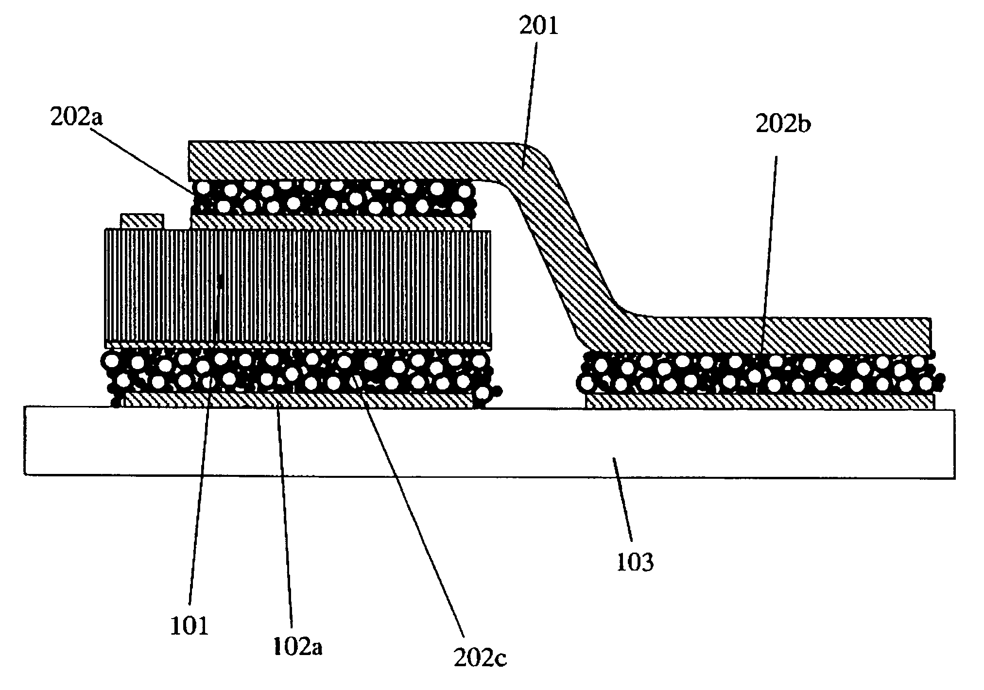
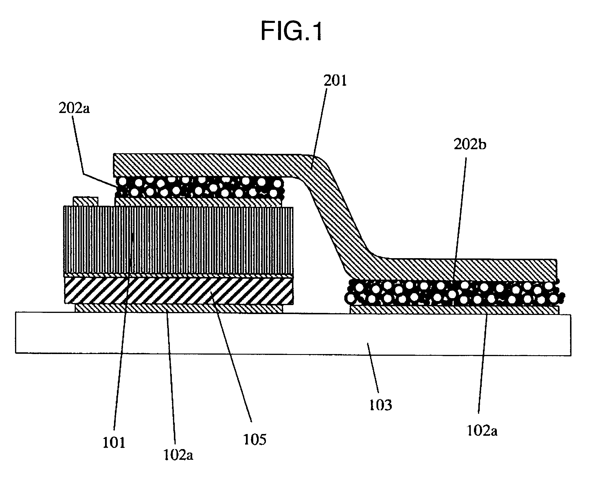
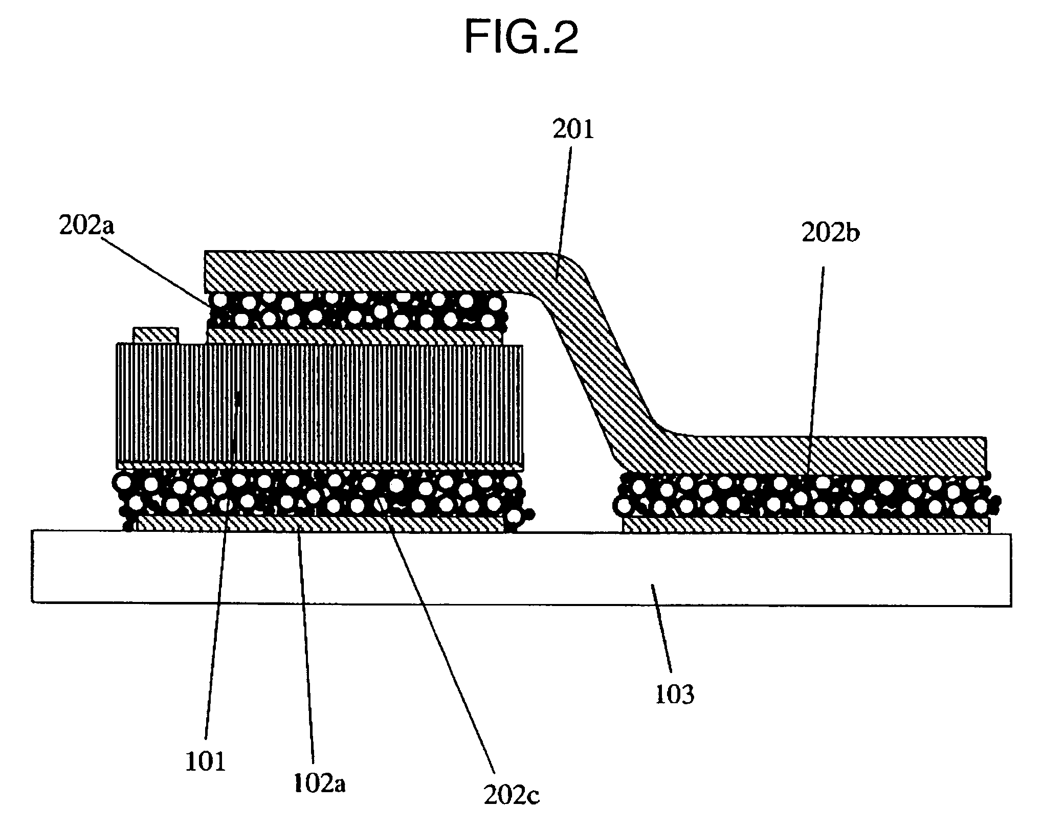
[0034]FIGS. 3A-3B and 4 depict one embodiment in case the invention is applied to an insulated type power semiconductor device for use in an inverter device, wherein FIG. 3A is a plan view, FIG. 3B is a sectional view along the line A-A′ of FIG. 3A, and FIG. 4 is a perspective view. In these drawings, reference numeral 101 designates semiconductor elements; 102a and 102b denote conductive layers; 103 indicates a ceramics insulating substrate; 110 is a supporting member; 111, a case; 112, external terminals; 113, bonding wires; 114, a sealing material. Additionally, the power semiconductor device per se is indicated by numeral 100.

[0035]Note here that the support member 110 is made up of a copper plate or an aluminum plate and is arranged to function as a member for supporting an entirety while also functioning as a heat conduction path when attached to...


PUM


Abstract

A semiconductor device which uses a semiconductor element having main current input / output electrodes, one and the other of which are extended up to a one surface and a remaining surface of a semiconductor chip respectively for causing one of the input / output electrodes to be contacted with a conductive layer of a insulating substrate, whereby the semiconductor element is supported on or above the insulating substrate. A conductive strip which is made of a composite material of carbon and aluminum or a composite material of carbon and copper is used for connection between the remaining input / output electrode of the semiconductor chip and the conductive layer of the insulating substrate.

Description

CROSS-REFERENCE TO RELATED APPLICATION[0001]The present application relates to subject matters described in a co-pending patent application Ser. No. 10 / 996,038 filed on Nov. 24, 2004 entitled “ELECTRIC PART MOUNTING METHOD, SEMICONDUCTOR MODULE, AND SEMICONDUCTOR DEVICE” and assigned to the assignees of the present application. The disclosures of this co-pending application are incorporated herein by reference.BACKGROUND OF THE INVENTION[0002]The present invention relates to semiconductor devices with relatively large power capacities and, more particularly, to a semiconductor device capable of offering enhanced performances even in high temperature environments, such as within an engine room or the like. This invention also relates to an electrical power converting device using the semiconductor device along with a hybrid vehicle using this power converter.[0003]In recent years, from standpoints of energy conservation and environmental pollution, the so-called hybrid vehicles which...

Claims


Application Information

Patent Timeline
Patent Type & Authority Patents(United States)
IPC IPC(8): H01L23/48H01L23/40H01L23/52
CPCH01L23/4928H01L23/49579H01L24/33H01L24/40H01L24/84H01L2924/1305H01L2924/1306H01L2224/49175H01L2224/49111H01L2224/48227H01L2224/45124H01L2224/29144H01L2224/29139H01L2224/29111H01L2924/1579H01L2924/15787H01L2924/0132H01L2924/19107H01L2924/014H01L2924/01033H01L2924/01023H01L2924/01006H01L2224/27505H01L2224/32225H01L2924/01005H01L2924/01013H01L2924/01027H01L2924/01029H01L2924/0103H01L2924/01047H01L2924/01049H01L2924/0105H01L2924/01051H01L2924/01074H01L2924/01078H01L2924/01079H01L2924/01082H01L2924/01322H01L2924/13055H01L2924/13091H01L2924/19041H01L2924/19043H01L2924/30105H01L2924/3512H01L2924/00H01L2924/00014H01L2924/351H01L2224/40095H01L2224/40225H01L2924/181H01L2224/73221H01L2224/84801H01L2224/3754H01L2224/37599H01L2224/371H01L24/37H01L2224/37124H01L2224/37147H01L2224/83801H01L2224/37298H01L2224/37666H01L2224/8384H01L2224/8484H01L2224/73263H01L2924/00012
Inventor MORITA, TOSHIAKIHOZOJI, HIROSHISUZUKI, KAZUHIRO
Owner HITACHI LTD
Why Eureka
Try Eureka