Switched converter with variable peak current and variable off-time control

a technology of switching converter and peak current, applied in the direction of electrical variable regulation, efficient power electronics conversion, instruments, etc., can solve the problems of poor light load efficiency and the emitted sound of ceramic capacitors, and achieve the effect of efficient operation

Active Publication Date: 2009-05-05
ANALOG DEVICES INT UNLTD
View PDF28 Cites 14 Cited by
  • Summary
  • Abstract
  • Description
  • Claims
  • Application Information

AI Technical Summary

Benefits of technology

[0014]Thus the regulator switch is continuously and adaptively controlled for successive activation and deactivation over a wide range of load conditions to provide efficient operation over the wide range while preventing the deactivation time of the switch from exceeding a predetermined level. The maximum switch off-time can be limited to a value, for example 25 μsec., so that switching frequency will not fall into the audio band. Traditional burst mode operation has been eliminated.

Problems solved by technology

The audio switching frequency can cause a ceramic capacitor to emit audio waves, which are undesirable to the end user of a system.
However, the efficiency at light load is poor as the switching frequency remains high during light load conditions.

Method used


Image

  • Switched converter with variable peak current and variable off-time control
  • Switched converter with variable peak current and variable off-time control
  • Switched converter with variable peak current and variable off-time control

Examples


Embodiment Construction

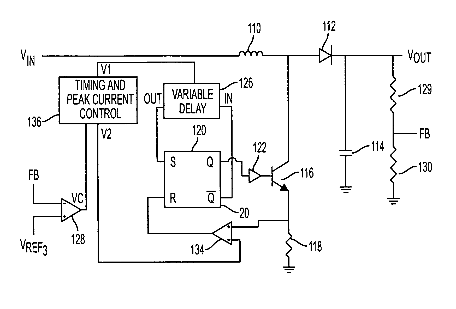
[0026]FIG. 3 is a block diagram of a boost switching regulator in accordance with an embodiment of the present invention. It should be understood that the principles described herein are applicable to boost, buck, and buck-boost current mode switching converters that can provide a regulated output voltage, at either polarity, of any particular desired level from any given DC source. Coupled in series between input node VIN and output node VOUT are inductor 110 and diode 112. Capacitor 114 is connected between the output node and ground. Signal responsive switch 116, shown as a transistor, and sensing resistor 118 are coupled in series between the junction of inductor 110 and diode 112, and ground. Coupled in series between the voltage output node and ground are resistors 129 and 130.

[0027]The base of transistor 116 is coupled to the Q output of latch 120 through switch driver circuit 122. Variable delay circuit 126 is coupled between the Q output of latch 120 and the set input of th...


PUM


Abstract

A converter coupled to a DC voltage input and connectable to a load, includes a signal responsive switch coupled between a first circuit point and a second circuit point. In lieu of burst mode operation during low load conditions, the peak switch current is varied directly with load condition and a switch deactivation interval is varied inversely with load condition. The switch deactivation level is within a maximum level to avoid audio frequency band interference, while maintaining high efficiency operation throughout the load range.

Description

TECHNICAL FIELD[0001]The disclosure relates to switched voltage regulators, more particularly to the control of peak current and switch off-time in accordance with sensed load condition.BACKGROUND[0002]The use of switching regulators to control a DC output voltage at a level higher than, lower than, or the same as, an input voltage is well known. Typically, one or more switches are activated to supply current pulses via an inductor to charge an output capacitor. The output voltage level is maintained at a desired level by adjusting the on and off times of the switching pulses in accordance with output voltage and load conditions.[0003]A conventional step-up, or boost, DC / DC converter is illustrated in FIG. 1. Inductor 10 and diode 12 are connected in series between input (VIN) and output (VOUT) nodes. The input node is typically connected to a DC source, the controlled output node coupled to a load. Capacitor 14 is connected between the output node and ground. Signal responsive swit...

Claims


Application Information

Patent Timeline
Patent Type & Authority Patents(United States)
IPC IPC(8): G05F1/00
CPCH02M3/1563H02M2001/0032Y02B70/16H02M1/0032H02M1/0035Y02B70/10G05F3/02
Inventor WU, ALBERT M.PIETKIEWICZ, STEVEN M.
Owner ANALOG DEVICES INT UNLTD
Why Eureka
Try Eureka