

Techniques for reconfiguring programmable circuit blocks
- Summary
- Abstract
- Description
- Claims
- Application Information
AI Technical Summary
Benefits of technology
Problems solved by technology
Method used
Image

Examples
Embodiment Construction
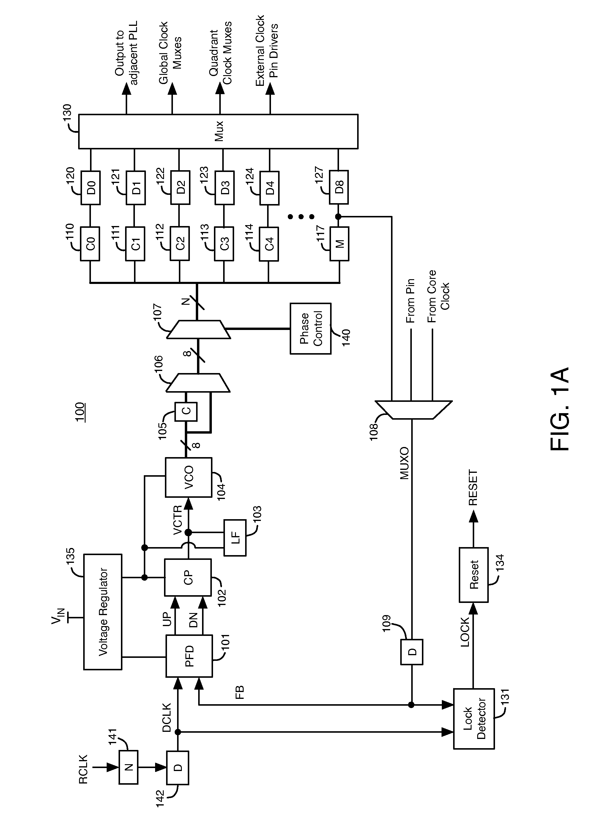
[0021]FIG. 1A illustrates a phase-locked loop (PLL) 100, according to an embodiment of the present invention. An input N counter circuit 141 receives an input reference clock signal RCLK at its input. RCLK is a periodic input signal. Counter 141 divides the frequency of RCLK by a frequency divider ratio N to generate an output signal. Delay circuit 142 delays the output signal of counter circuit 141 to generate clock signal DCLK. Delay circuit 142 has a programmable delay. The delay of delay circuit 142 can be programmed to compensate for any offsets in PLL 100.
[0022]The divided and delayed clock signal DCLK is transmitted to a first input of a phase frequency detector (PFD) 101. PFD 101 compares the phase and frequency of clock signal DCLK to the phase and frequency of a feedback clock signal FB to generate pulses in UP and DN output signals.
[0023]The UP and DN signals are transmitted to inputs of charge pump (CP) circuit 102. PFD 101 generates longer high pulses in the UP signal w...
PUM
 Abstract
Description
Claims
Application Information