Manufacturing method of semiconductor integrated circuit device

a manufacturing method and integrated circuit technology, applied in the direction of individual semiconductor device testing, semiconductor/solid-state device testing/measurement, instruments, etc., can solve the problem of difficult to match the installation of the probe stylus with the arranged position of the test pad to be probed, and achieve the effect of enhancing the yield of collectively performing probes on a plurality of chips

Inactive Publication Date: 2009-05-19
RENESAS ELECTRONICS CORP
View PDF11 Cites 3 Cited by
  • Summary
  • Abstract
  • Description
  • Claims
  • Application Information

AI Technical Summary

Benefits of technology

[0012]In recent years, multi-functionalization of semiconductor integrated circuit devices has so much progressed that even a plurality of circuits are built into a single semiconductor chip (hereinafter referred to as simply “chip”). Further, with a view to suppressing the manufacturing cost of semiconductor integrated circuit devices, attempts are being made to miniaturize semiconductor elements and wiring to reduce the area of a semiconductor chip (hereinafter referred to as simply “chip”) and to increase the number of chips acquired per semiconductor wafer (hereinafter referred to as simply “wafer”). For this purpose, not only the number of test pads (bonding pads) is increased, but the test pads are arranged at a narrower pitch and the areas of test pads are reduced. Along with this pitch narrowing of test pads, where a prober having cantilever-shaped probe styluses is to be used for the probing, there arises a problem that it is difficult to install the probe styluses matched with the arranged positions of the test pads to be probed.
[0016]Adjusting the membrane probe or the like to improve the differences among the depressions in distinctiveness by uniformizing the contact pressures between the probe styluses and the respectively matching test pads would take a long time as well as a high skill level.
[0023]The object of one typical aspect of the invention disclosed in this application is to provide a technique by which the yield of probing, applied collectively to a plurality of chips, can be enhanced by using a membrane probe by using a manufacturing technique for semiconductor integrated circuit devices.
[0024]The object of another typical aspect of the invention disclosed in this application is to reduce the length of time taken to perform probing in a manufacturing process of semiconductor integrated circuit devices.
[0170]25. A wafer process resembling stylus, a stylus for wiring integrated sheets, a probe card using a wiring integration process (a combination of a probing stylus, wiring integrated sheet assembly, namely a stylus, wiring integrated thin-film sheet and a mechanism to hold them, tap wiring and so forth) for use in fabricating semiconductor integrated circuit devices, wherein the stylus and wiring integrated sheet include a plurality of sub-sheets (or fabrication of a plurality of probe cards by separating a plurality of sub-sheets from single sheets enables probe cards of relatively small areas to be easily prepared).
[0180]By using a membrane probe formed by using a manufacturing technique for semiconductor integrated circuit devices, the yield of probing collectively performed on a plurality of chips can be enhanced.

Problems solved by technology

Along with this pitch narrowing of test pads, where a prober having cantilever-shaped probe styluses is to be used for the probing, there arises a problem that it is difficult to install the probe styluses matched with the arranged positions of the test pads to be probed.

Method used


Image

  • Manufacturing method of semiconductor integrated circuit device
  • Manufacturing method of semiconductor integrated circuit device
  • Manufacturing method of semiconductor integrated circuit device

Examples


embodiment 1

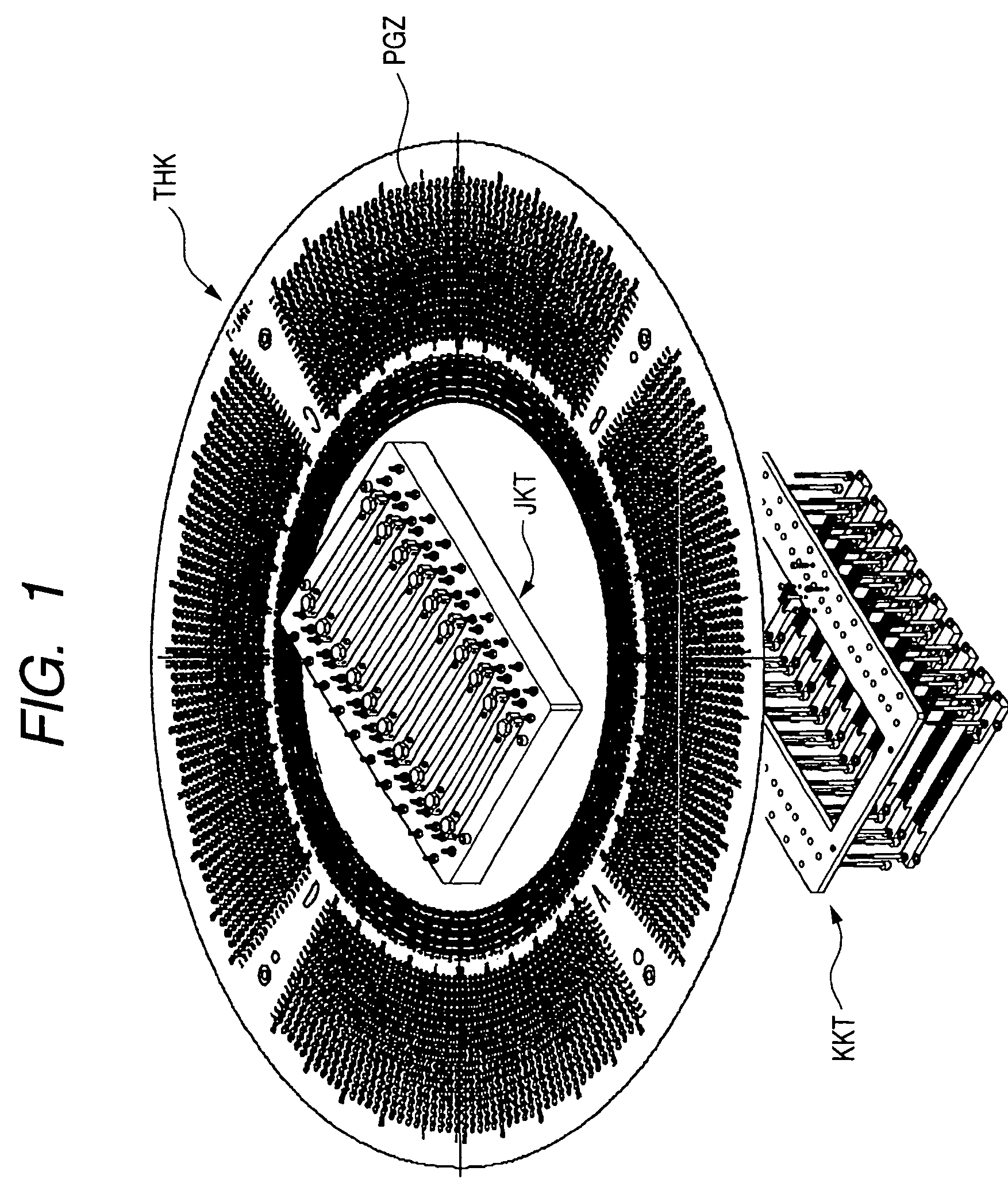
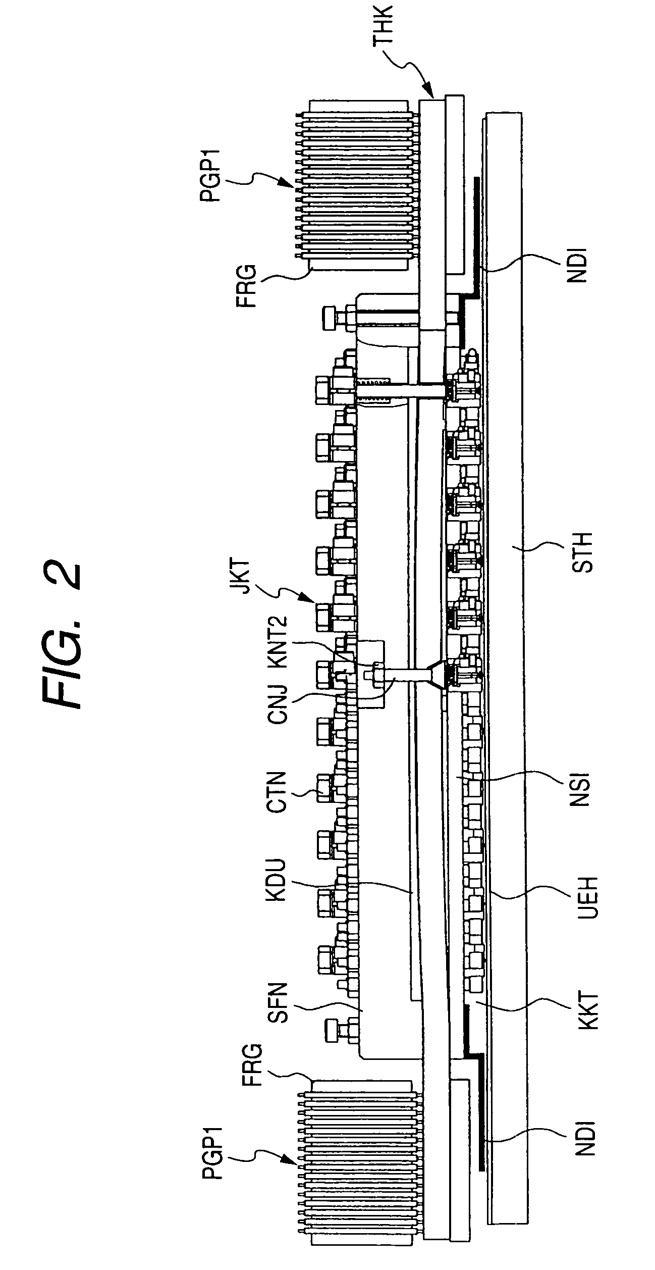
[0241]FIG. 1 is a perspective view of the structure of a probe card in this Embodiment 1. FIG. 2 is a sectional view of the essential parts of that probe card. FIG. 3 is a perspective view illustrating the structure of an upper structural unit and a lower structural unit which make up part of components constituting that probe card. FIG. 4 is a top view of that upper structural unit 3. FIG. 5 is a bottom view of that lower structural unit.

[0242]The probe card of this Embodiment 1 is composed by fitting an upper structural unit JKT from above and a lower structural unit KKT from underneath to a multi-layer wiring substrate THK. The lower structural unit KKT has a thin-film sheet (membrane probe), and a plurality of probes and a plurality of wirings each electrically connected to one or another of the plurality of probes are formed on that thin-film sheet. The plurality of wirings are electrically connected via a wiring (first wiring) formed within the multi-layer wiring substrate THK...

embodiment 2

[0316]The foregoing Embodiment 1 has a structure in which the POGO pins PGP2 press the elastomers 48 on the probes 7A (see FIG. 6 and FIG. 8), but this Embodiment 2 has a structure in which the POGO pins PGP2 press both of the metal films 45 so arranged as hold those elastomers 48 between them and those elastomers 48 are dispensed with. In all other respects, this embodiment is the same as the foregoing Embodiment 1. FIG. 35 is a perspective view of a POGO pin insulator PIL2 of this Embodiment 2 holding the POGO pins PGP2 and FIG. 36, a sectional view, in a state in which the POGO pin insulator PIL2 is incorporated into the adhesive holder SHD, of a structural unit which they constitute.

[0317]The POGO pin insulator PIL2 is the same as the POGO pin insulator PIL1 in the foregoing Embodiment 1 except in the position and the number of the POGO pins PGP2 it holds.

[0318]In this Embodiment 2, more of the POGO pins PGP2 are arranged than in the foregoing Embodiment 1. This feature enables ...

embodiment 3

[0320]The probe card of this Embodiment 3 has a pusher different in structure from the pusher PSY (see FIG. 6 and FIG. 8) in the probe card of the foregoing Embodiment 1.

[0321]FIG. 37 is a perspective view illustrating the structure of the pusher PSY of this Embodiment 3 and FIG. 38, a sectional view of the essential parts thereof.

[0322]In this Embodiment 3, pressing mechanisms OAJ of sizes matching individual chips CHP are used, as shown in FIG. 37, in place of the POGO pin insulator PIL1 in the foregoing Embodiment 1. These pressing mechanisms OAJ, are formed of ceramic for instance. A one-side driven type POGO pin PGP3 is inserted into a hole AN1 bored in the pressing mechanism OAJ, and the pressing of the pressing mechanism OAJ by this POGO pin PGP3 causes the tip of the pressing mechanism OAJ to press the part of the membrane probe HMS in which the probes 7A are formed. A thin elastomer sheet ESS, arranged between the pressing mechanism OAJ and the membrane probe HMS, performs ...


PUM


Abstract

By using a membrane probe formed by using a manufacturing technique for semiconductor integrated circuit devices, the yield of probing collectively performed on a plurality of chips is to be enhanced. A probe card is formed by using a plurality of pushers, each pusher being formed of a POGO pin insulator, POGO pins, an FPC connector, a membrane probe HMS, an impact easing sheet, an impact easing plate, a chip condenser YRS and so on, wherein one or two POGO pins press a plurality of metal films arranged like islands. One or more cuts are made into what matches the chip to be tested in the area of the membrane probe in a direction substantially parallel to the extending direction of wiring electrically connected to probes formed in the membrane probe.

Description

BACKGROUND OF THE INVENTION[0001]The present invention relates to a manufacturing method of semiconductor integrated circuit devices, and more particularly to a technique that can be effectively applied to electrical testing of semiconductor integrated circuit devices which is performed by pressing the probe styluses of a probe card against the electrode pads of each semiconductor integrated circuit device.[0002]In each of Japanese Unexamined Patent Publication No. Hei 7(1995)-283280 (Patent Document 1), Japanese Unexamined Patent Publication No. Hei 8(1996)-50146 (Patent Document 2 (corresponding PCT: International Publication WO 95-34000)), Japanese Unexamined Patent Publication No. Hei 8(1996)-201427 (Patent Document 3), Japanese Unexamined Patent Publication No. Hei 10(1998)-308423 (Patent Document 4), Japanese Unexamined Patent Publication No. Hei 11(1999)-23615 (Patent Document 5 (corresponding U.S. Patent publication: U.S. Pat. No. 6,305,230)), Japanese Unexamined Patent Publ...

Claims


Application Information

Patent Timeline
Patent Type & Authority Patents(United States)
IPC IPC(8): H01L21/66
CPCG01R1/0735H01L22/00
Inventor SHOJI, TERUOHASEBE, AKIODEGUCHI, YOSHINORIMURAKAMI, MOTOJIOKAMOTO, MASAYOSHINARIZUKA, YASUNORIKASUKABE, SUSUMU
Owner RENESAS ELECTRONICS CORP
Why Eureka
Try Eureka