Gate structure and method

a gate structure and gate technology, applied in the field of electronic semiconductor devices, can solve the problems of poor interface stability of materials with silicon, leakage current problems, and silicate dielectrics, and achieve the effect of limiting the reaction of silicate gate dielectri

Active Publication Date: 2009-05-19
TEXAS INSTR INC
View PDF8 Cites 9 Cited by
  • Summary
  • Abstract
  • Description
  • Claims
  • Application Information

AI Technical Summary

Benefits of technology

[0007]This has advantages including limiting reaction of silicate gate dielectric with gate material.

Problems solved by technology

However, such thin oxides present leakage current problems due to carrier tunneling through the oxide.
Indeed, Ta2O5, (Ba,Sr)TiO3, and other high dielectric constant materials have been suggested, but such materials have poor interface stability with silicon.
However, such silicate dielectrics have problems with high volume production of silicon integrated circuits such as reactivity with the subsequently deposited gate material.

Method used


Image

  • Gate structure and method
  • Gate structure and method
  • Gate structure and method

Examples


Embodiment Construction

1. Overview

[0010]Preferred embodiment integrated circuits and MOS transistors include metal silicate gate dielectrics and / or metal gates with differing work functions within the same integrated circuit. Preferred embodiment fabrication methods include treatments of a substrate surface prior to gate dielectric deposition, treatment of a gate dielectric surface prior to deposition of gate material, metal gates of two different metals or textures on the same integrated circuit, . . .

2. Silicon Gate with Silicate Gate Dielectric Preferred Embodiments

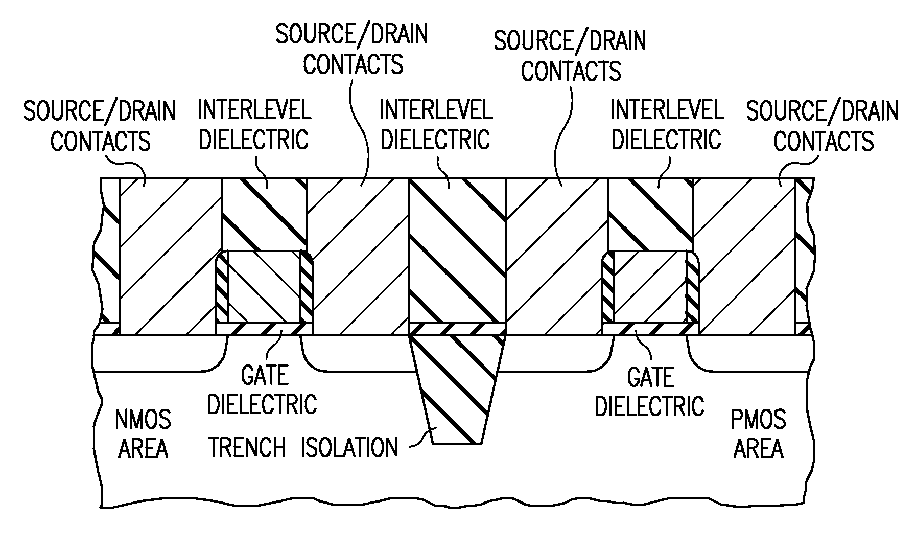
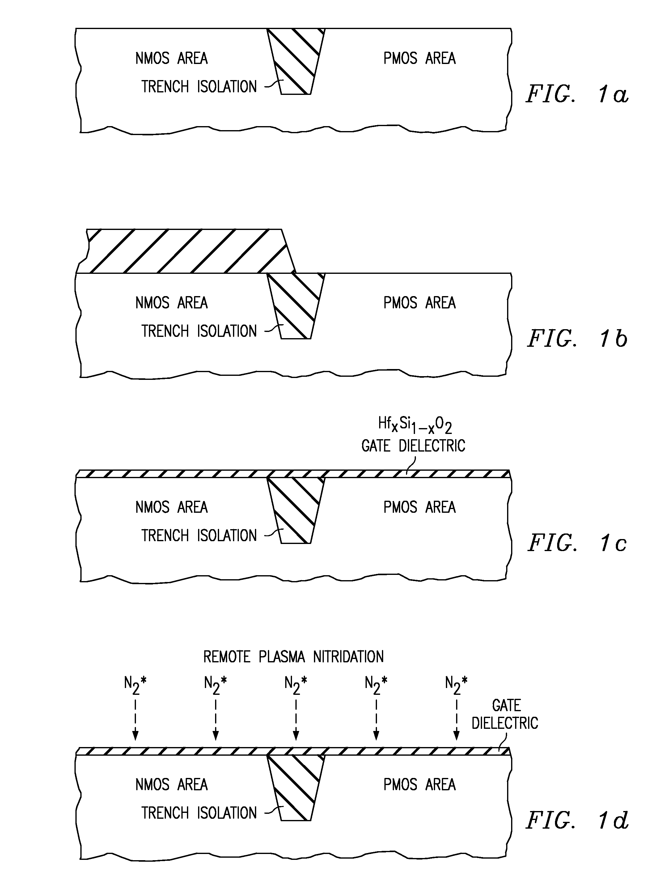
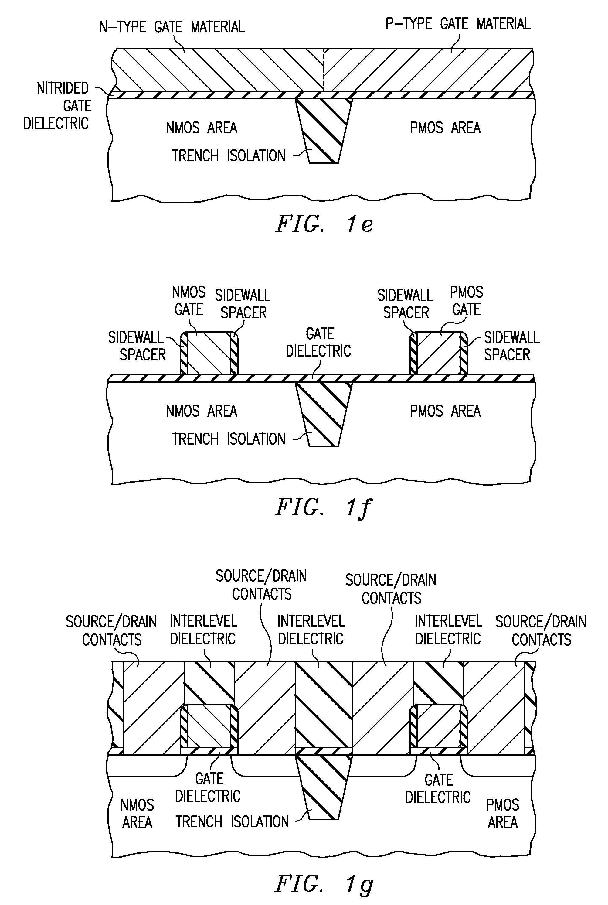
[0011]FIGS. 1a-1m illustrate in cross sectional elevation views the steps of first preferred embodiment fabrication methods for integrated circuits including field effect transistors (e.g., CMOS or BiCMOS) with silicate gate dielectrics and polysilicon gates. The preferred embodiments include the following steps:

[0012](1) Substrate.

[0013]Start with a p-type silicon (or silicon-on-insulator) wafer with orientation and form shallow trench iso...


PUM


Abstract

A MOSFET structure including silicate gate dielectrics with nitridation treatments of the gate dielectric prior to gate material deposition.

Description

RELATED APPLICATIONS[0001]This application claims priority from provisional patent application Ser. No. 60 / 351,323, filed Jan. 23, 2002. The following patent applications disclose related subject matter: U.S. Ser. No. 10 / 232,124 filed Aug. 30, 2002 . These applications have a common assignee with the present application.BACKGROUND OF THE INVENTION[0002]The invention relates to electronic semiconductor devices, and, more particularly, to gate structures and fabrication methods for integrated circuits.[0003]The trend in semiconductor integrated circuits to higher device densities by down-scaling structure sizes and operating voltages has led to silicon field effect (MOS) transistor gate dielectrics, typically made of silicon dioxide, to approach thicknesses on the order of 1-2 nm to maintain the capacitive coupling of the gate to the channel. However, such thin oxides present leakage current problems due to carrier tunneling through the oxide. Consequently, alternative gate dielectric...

Claims


Application Information

Patent Timeline
Patent Type & Authority Patents(United States)
IPC IPC(8): H01L29/76H01L29/94H01L21/28H01L21/8238H01L27/092H01L29/51
CPCH01L21/28194H01L21/28202H01L21/823857H01L21/823871H01L27/092H01L29/517H01L29/518
Inventor ROTONDARO, ANTONIO L. P.COLOMBO, LUIGIVISOKAY, MARK R.KHAMANKAR, RAJESHMERCER, DOUGLAS E.
Owner TEXAS INSTR INC
Why Eureka
Try Eureka