Chip embedded packaging structure

a technology of embedded packaging and chips, applied in the direction of printed capacitor incorporation, association of printed circuit non-printed electric components, electrical apparatus construction details, etc., can solve problems such as electrical performance of devices, and achieve the effects of reducing noise, shortening wiring distance, and increasing overall electrical performan

Active Publication Date: 2009-05-26
PHOENIX PRECISION TECH CORP
View PDF6 Cites 13 Cited by
  • Summary
  • Abstract
  • Description
  • Claims
  • Application Information

AI Technical Summary

Benefits of technology

[0009]Overall, the chip embedded packaging structure comprising active or passive chips includes the following advantages:
[0011]b) Achieves grounding effect by connecting the active and passive chips to the heat dissipation substrate to increase overall electrical performance and reduce noise.
[0012]c) Shortens wiring distance, reduces product size, and increases product performance, thereby achieving multi-functionality by integrating active and passive chips into the substrate and forming an MIM capacitor via the passive component layer.

Problems solved by technology

Nevertheless, the flip chips and passive components connected to the surface of the multi-layer circuit board still have to be electrically connected via the circuit layer embedded within the circuit board, and overly long distances between a connection will often influence the electrical performance of the device.

Method used


Image

  • Chip embedded packaging structure
  • Chip embedded packaging structure
  • Chip embedded packaging structure

Examples


Embodiment Construction

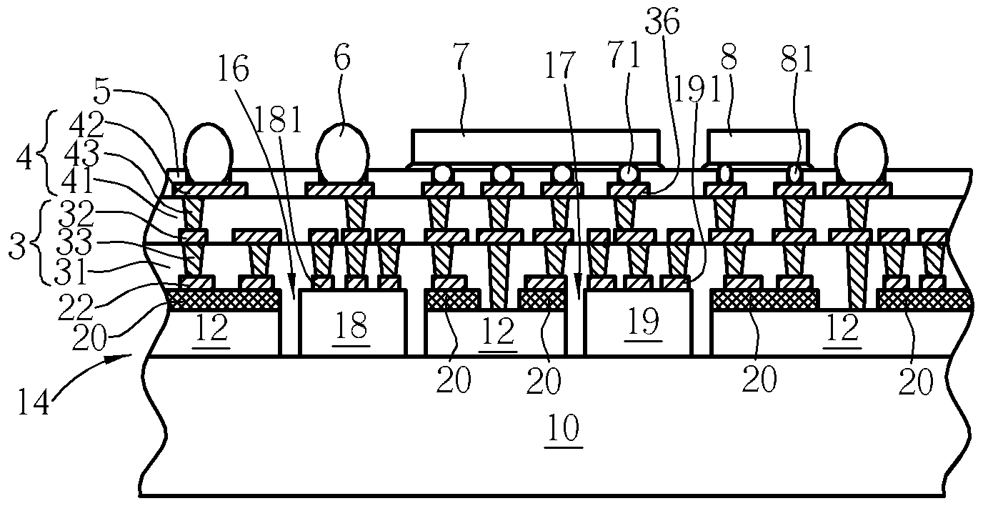
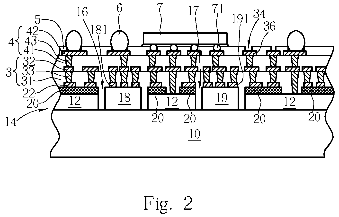
[0018]Please refer to FIG. 1. FIG. 1 is a perspective diagram showing the cross section of the chip embedded packaging structure containing embedded active and passive chips according to the preferred embodiment of the present invention. As shown in FIG. 1, the bottom of the structure includes a first metal board 10, and a second metal board 12 is disposed on the upper surface of the first metal board 10, in which the second metal board 12 and the first metal board 10 together form a heat dissipating substrate 14. Preferably, the second metal board 12 includes at least a through cavity, such as cavity 16 and 17, and the first metal board 10 and the second metal board 12 can be composed of same or different material. For instance, an etching process can be performed to form a cavity with a predetermined depth on a metal board, such as forming the first metal board 10 and the second metal board 12 with a through cavity. Alternatively, a metal layer containing a through cavity can be f...


PUM


Abstract

A chip embedded packaging structure includes a first metal board, a second metal board having at least a through cavity, in which the second metal board is disposed on the upper surface of the first metal board to form a heat dissipating substrate, at least a semiconductor chip and a capacitor chip embedded in the first metal board and embraced in the through cavity of the second metal board, a passive component layer disposed on part of the upper surface of the second metal board, and at least a build-up circuit layer covering the semiconductor chip, the capacitor chip, and the passive component layer and electrically connecting them through a plurality of conductive vias.

Description

BACKGROUND OF THE INVENTION[0001]1. Field of the Invention[0002]The present invention relates to a chip embedded packaging structure, and more particular to a chip embedded packaging structure containing active and passive chips between a build-up circuit layer and a heat dissipating substrate.[0003]2. Description of the Prior Art[0004]In recent years, as information appliances and communication products develop and the capacity of information transmission expands, the demand for higher signal transmission also increases accordingly. At the same time, under the popularity of hand-held electronic products, the development of semiconductor fabrication processes is moving toward the direction of high capacity, high frequency, low power consumption, and multi-functional integration.[0005]Under the field of IC packaging techniques, the complexity of various types of IC packages including the chip scale package (CSP) and the flip chip (FC) package have also increased significantly to acco...

Claims


Application Information

Patent Timeline
Patent Type & Authority Patents(United States)
IPC IPC(8): H05K1/18
CPCH01L23/5389H01L24/82H01L25/16H05K1/185H01L24/24H01L2224/16235H01L2224/16225H01L2224/24227H01L2224/73204H01L2924/14H01L2924/15153H01L2924/1517H01L2924/15311H01L2924/1532H01L2924/19041H05K1/0203H05K1/05H05K1/162H05K3/4644H05K2201/09554H05K2201/09745H01L2224/32225H01L2924/014H01L2924/01033H01L2924/01006H01L2924/01005H01L2924/00H01L24/19H01L2224/04105H01L2224/12105H01L2224/16227H01L2224/32245H01L2224/73267H01L2924/19105
Inventor HSU, SHIH-PING
Owner PHOENIX PRECISION TECH CORP
Why Eureka
Try Eureka