Method for manufacturing semiconductor device and MOS field effect transistor

a technology of mos field effect transistor and semiconductor device, which is applied in the direction of semiconductor devices, basic electric elements, electrical equipment, etc., can solve the problems of increasing the off-leakage current of the soi-mosfet, and reducing the drain breakdown voltage. , to achieve the effect of reducing the off-leakage current and suppressing the floating body

Inactive Publication Date:
View PDF9 Cites 0 Cited by
  • Summary
  • Abstract
  • Description
  • Claims
  • Application Information

AI Technical Summary

Benefits of technology

[0042]That is, in the present invention, the recovery of some of the crystal defects and the activation of the first dopant both of which have heretofore been simultaneously performed at one anneal, are respectively carried out in discrete process steps (high-temperature anneal and anneal). Thus, since the first dopant is not yet introduced in the device forming area at the stage of execution of the high-temperature anneal for recovery of some of the crystal defects, there is no fear of excessive diffusion of the first dopant along a gate-length direction, and the high-temperature anneal can be carried out at the optimum temperature (temperature higher than an anneal temperature for activation of the first dopant, to be described later) for recovering some of the crystal defects.
[0043]At the stage of execution of the anneal for activation of the first dopant, the crystal defects have already been recovered by the high-temperature anneal. Therefore, anneal can be performed at the optimum temperature (temperature lower than the above high-temperature anneal temperature) enabling the activation of the first dopant while the excessive diffusion of the first dopant along the gate-length direction is being suppressed, without taking into consideration the recovery of the crystal defects. Thus, according to the manufacturing method of the semiconductor device according to the present invention, there can be provided a semiconductor device which simultaneously attains (1) suppression of floating body effects and (2) a reduction in off-leakage current at practically sufficient levels.
[0044]The MOS field effect transistor of the present invention attains (1) the suppression of floating body effects and a reduction in off-leakage current simultaneously at the practically sufficient levels while a short channel effect is being suppressed, regardless of the provision of the crystal defects defined as the recombination centers artificially introduced in the body region.

Problems solved by technology

Described more specifically, the holes are not able to escape to a source region due to an energy barrier between the source region and the channel region, thus resulting in the storage thereof in the channel region.
Problems such as the single latch up, the reduction in the drain breakdown voltage with the latch up, etc. come to the fore where the voltage applied to the drain region is high.
With the recent miniaturization of a semiconductor device, however, a new problem also arises with derivation from the crystal defects.
The new problem resides in an increase in off-leakage current of the SOI-MOSFET.
When, however, the anneal temperature is lowered, crystal defects derived from ion implantation of Ar are not recovered sufficiently, and a large number of crystal defects remain in the silicon semiconductor layer.
As result, a current leaks between the source regions and the drain region through the crystal defects in the SOI-MOSFET.
This results from floating body effects.
This means that in the case of the above anneal (975° C. for 10 seconds), the crystal effects derived from the Ar ion-implantation are not recovered sufficiently, and a current leaks between a source region and a drain region through the crystal defects.
It has been revealed from this that the mere decrease in the ion-implantation rate of Ar encounters difficulties in simultaneously attaining the suppression of the floating body effects and the reduction in the off-leakage current Idoff.

Method used


Image

  • Method for manufacturing semiconductor device and MOS field effect transistor
  • Method for manufacturing semiconductor device and MOS field effect transistor
  • Method for manufacturing semiconductor device and MOS field effect transistor

Examples


Embodiment Construction

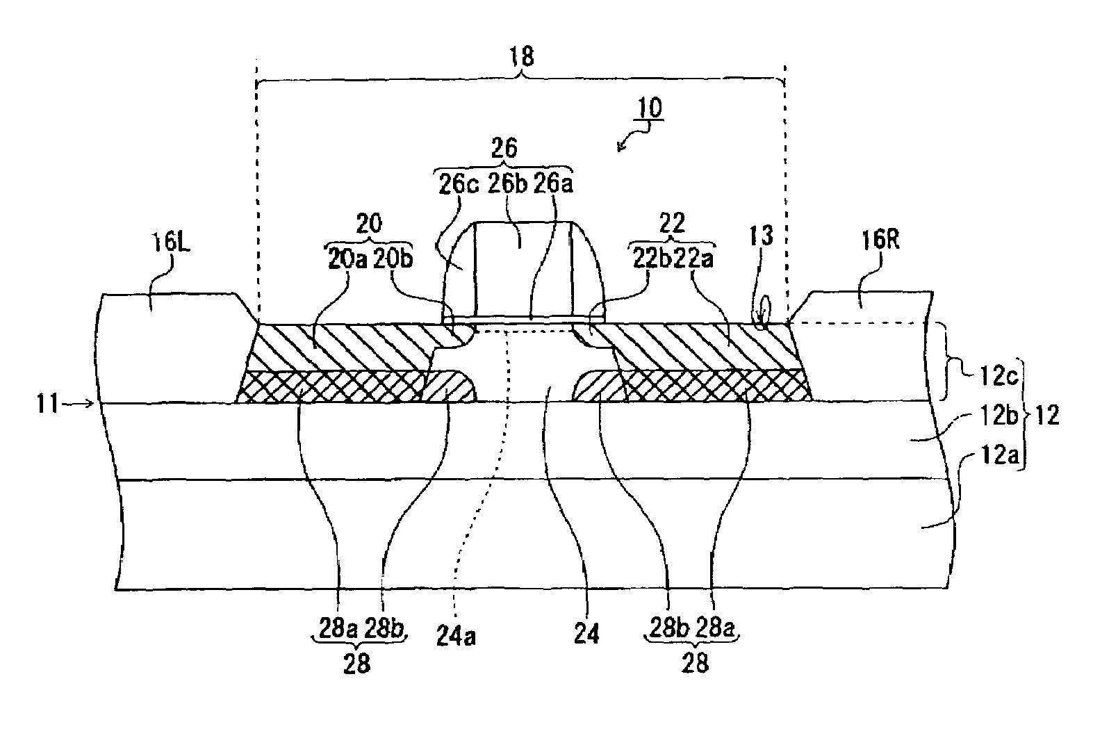
[0053]Preferred embodiments of the present invention will hereinafter be described with reference to the accompanying drawings. The shape, size and layout relationship of each constituent element in the figures are merely approximate illustrations to enable an understanding of the present invention. While preferred configurational examples of the present invention are explained below, the material and numerical conditions of each constituent element, etc. are nothing more than mere preferred examples. Accordingly, the present invention is by no means limited to an embodiment to be described below.

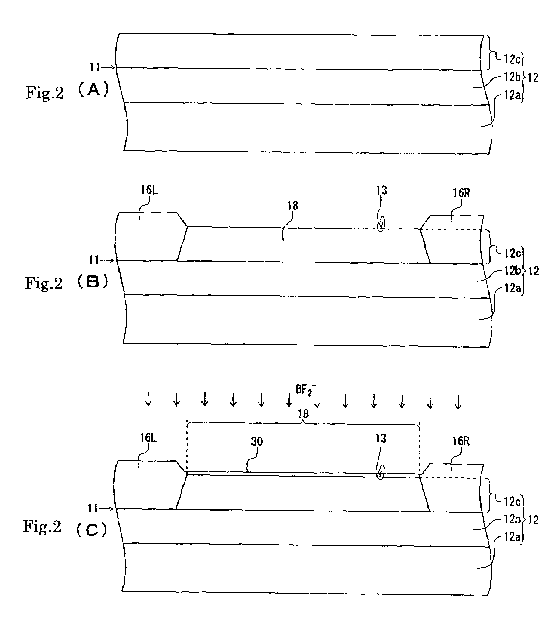
[0054]FIG. 1 is a view showing a cut area of a cross-section showing a schematic configuration of a semiconductor device according to the present embodiment. FIGS. 2(A), 2(B) and 2(C) are respectively views showing cut areas of cross-sections of such structures as obtained in major process steps of a method for manufacturing the semiconductor device according to the embodiment. FIGS. 3(A), ...


PUM


Abstract

Upon manufacture of a semiconductor device provided with a source region and a drain region formed by activating, through anneal, an n-type first dopant ion-implanted in a p-type device forming area provided in a semiconductor layer formed on an insulator, and a body region, (a) ion implantation of Ar in a boundary region between the source and drain regions to be formed, which corresponds to a region lying in a predeterminate area for forming the body region, and (b) high-temperature anneal for partly recovering crystal defects produced by the ion implantation of the Ar at a temperature higher than the anneal for activation of the first dopant are carried out prior to the ion-implantation of the first dopant.

Description

BACKGROUND OF THE INVENTION[0001]The present invention relates to a method for manufacturing a semiconductor device formed in a semiconductor layer provided on an insulator, and a MOS field effect transistor formed in a semiconductor layer provided on an insulator.[0002]There has heretofore been known a so-called SOI integrated circuit wherein an elemental device such as a transistor is formed in a silicon semiconductor layer by using an SOI (Silicon On Insulator) substrate in which the silicon semiconductor layer is laminated on an insulator.[0003]The SOI integrated circuit is superior to an integrated circuit (hereinafter called “silicon integrated circuit”) formed in a single silicon substrate in that, for example, (1) it is small in parasitic capacitance and excellent in high-speed performance, (2) it is resistant to soft errors, (3) no latch up occurs and (4) a well process can be omitted.[0004]In the SOI integrated circuit, particularly, a MOS field effect transistor (hereinaf...

Claims


Application Information

Patent Timeline
Patent Type & Authority Patents(United States)
IPC IPC(8): H01L21/84
CPCH01L29/66772H01L29/78612
Inventor DOMAE, YASUHIRO
Why Eureka
Try Eureka