Fabricating nanoscale and atomic scale devices

a technology of atomic scale and nano-scale, which is applied in the testing/measurement of individual semiconductor devices, semiconductor/solid-state devices, instruments, etc., to achieve the effect of accurately controlling the position of dopants and robust semiconductor devices

Active Publication Date: 2009-06-16
NEWSOUTH INNOVATIONS PTY LTD
View PDF7 Cites 13 Cited by
  • Summary
  • Abstract
  • Description
  • Claims
  • Application Information

AI Technical Summary

Benefits of technology

[0055]The registration markers survive all the process steps involved in the fabrication of the device. These steps might include flashing the surface to temperatures >1000° C., terminating the surface with a monolayer of hydrogen, selectively desorbing hydrogen atoms with either the STM tip with or without a scanning electron microscope (SEM) to pattern the device structure, dosing the exposed silicon surface with a dopant containing source, such as phosphine gas and encapsulating the resulting device. The invention is able to produce a robust semiconductor device, where the active component of the device is patterned by the STM. Given that we have also recently demonstrated that it is possible to dope silicon with atomic precision with a STM, the door is now open to the creation of fully functional nano and atomic scale silicon devices with both ohmic and control gate electrodes. This promises to open entirely new areas of quantum device physics, due to the ability to accurately control the position of dopants with atomic precision, and integrate quantum physics into device design (with applications for atomic-scale transistors, stub tuners, resonant tunnel diodes, etc).

Problems solved by technology

A difficulty arises when the patterned conducting region is not visible, for instance it may be encapsulated under several tens to hundreds of nanometers of silicon and therefore be invisible to optical and electron beam microscopes.
In this case, the challenge is to find a way to register the, perhaps atomically accurate, patterned conducting region to the silicon surface.

Method used


Image

  • Fabricating nanoscale and atomic scale devices
  • Fabricating nanoscale and atomic scale devices
  • Fabricating nanoscale and atomic scale devices

Examples


Embodiment Construction

The Fabrication Approach

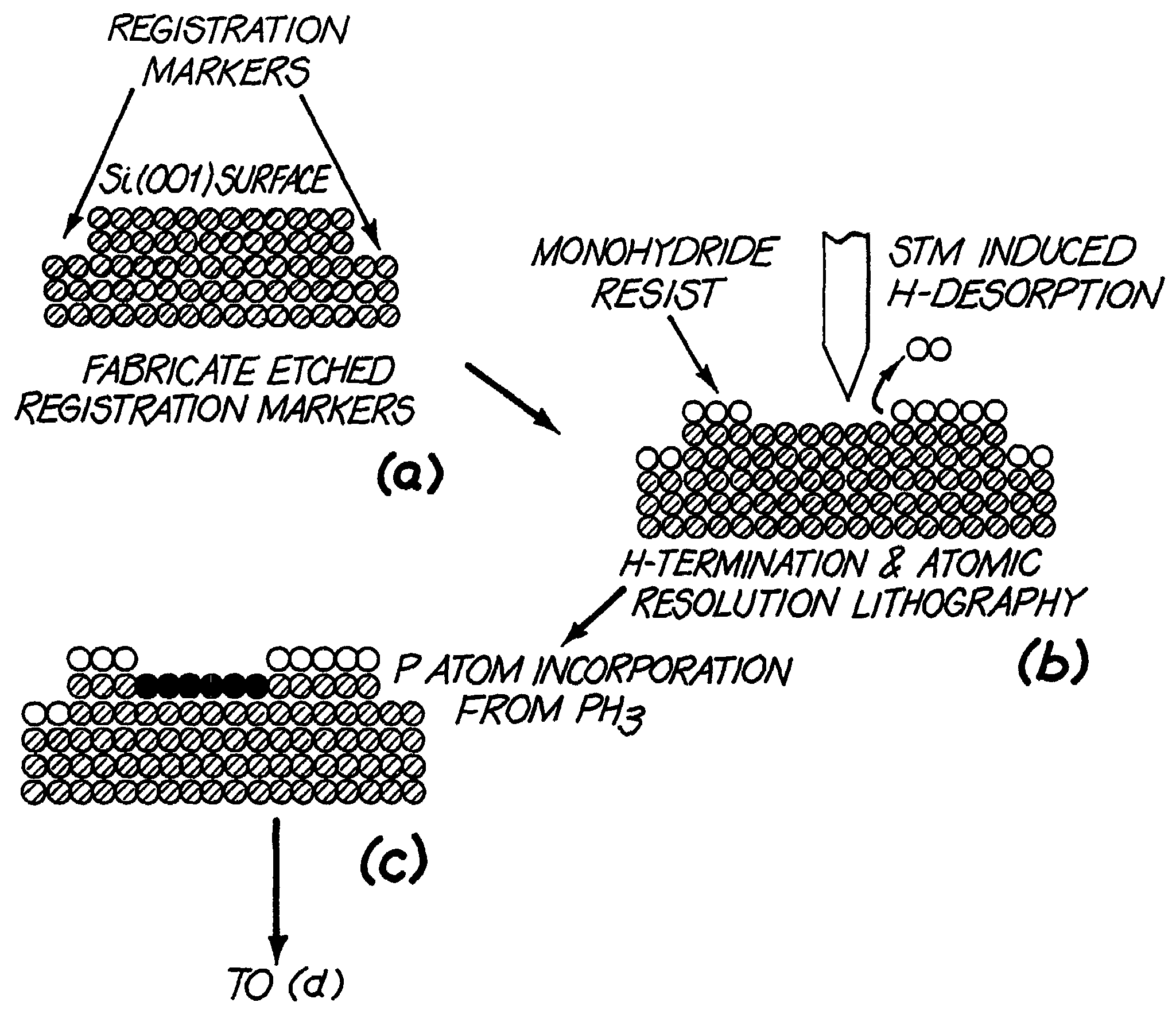
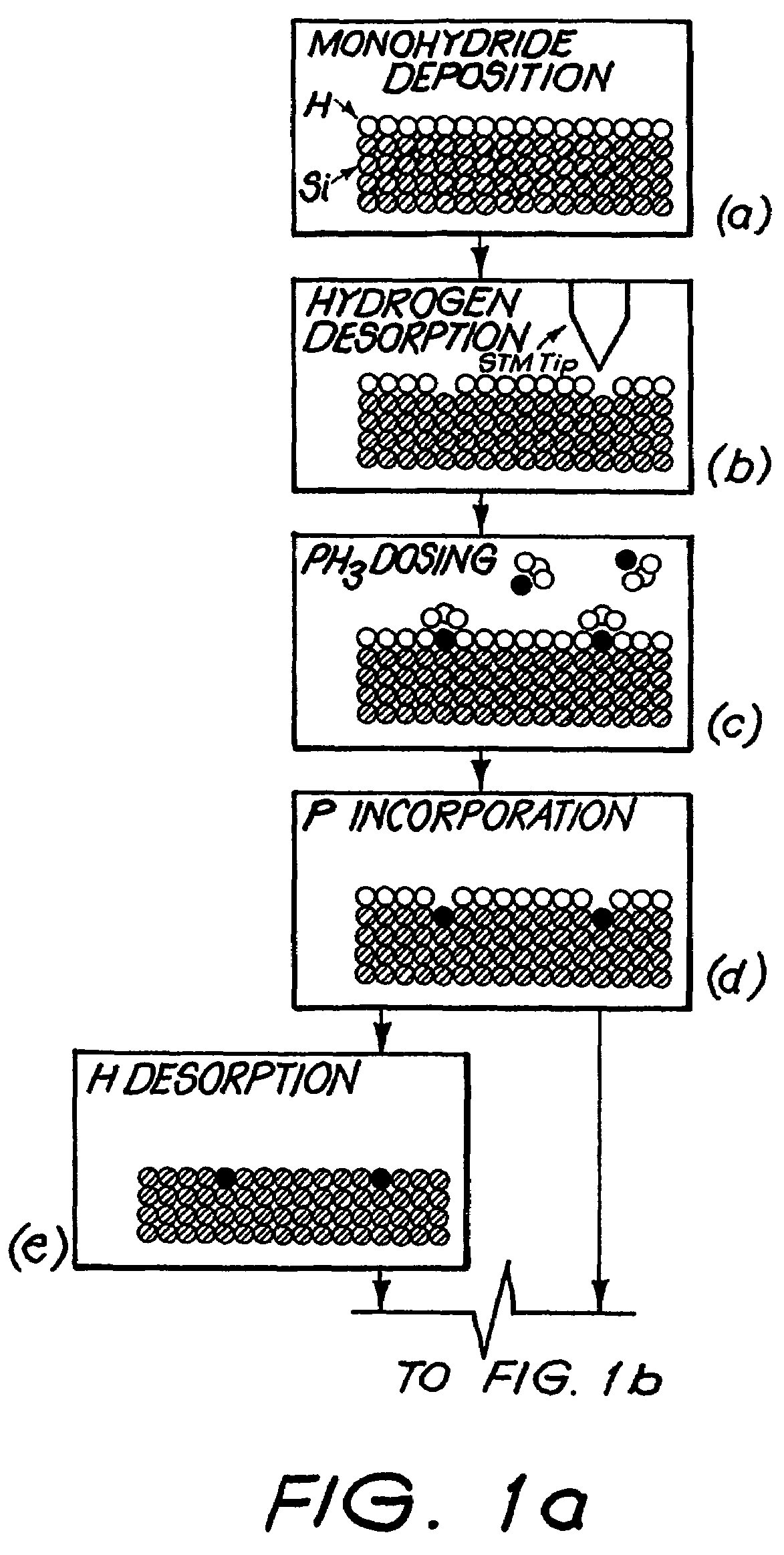
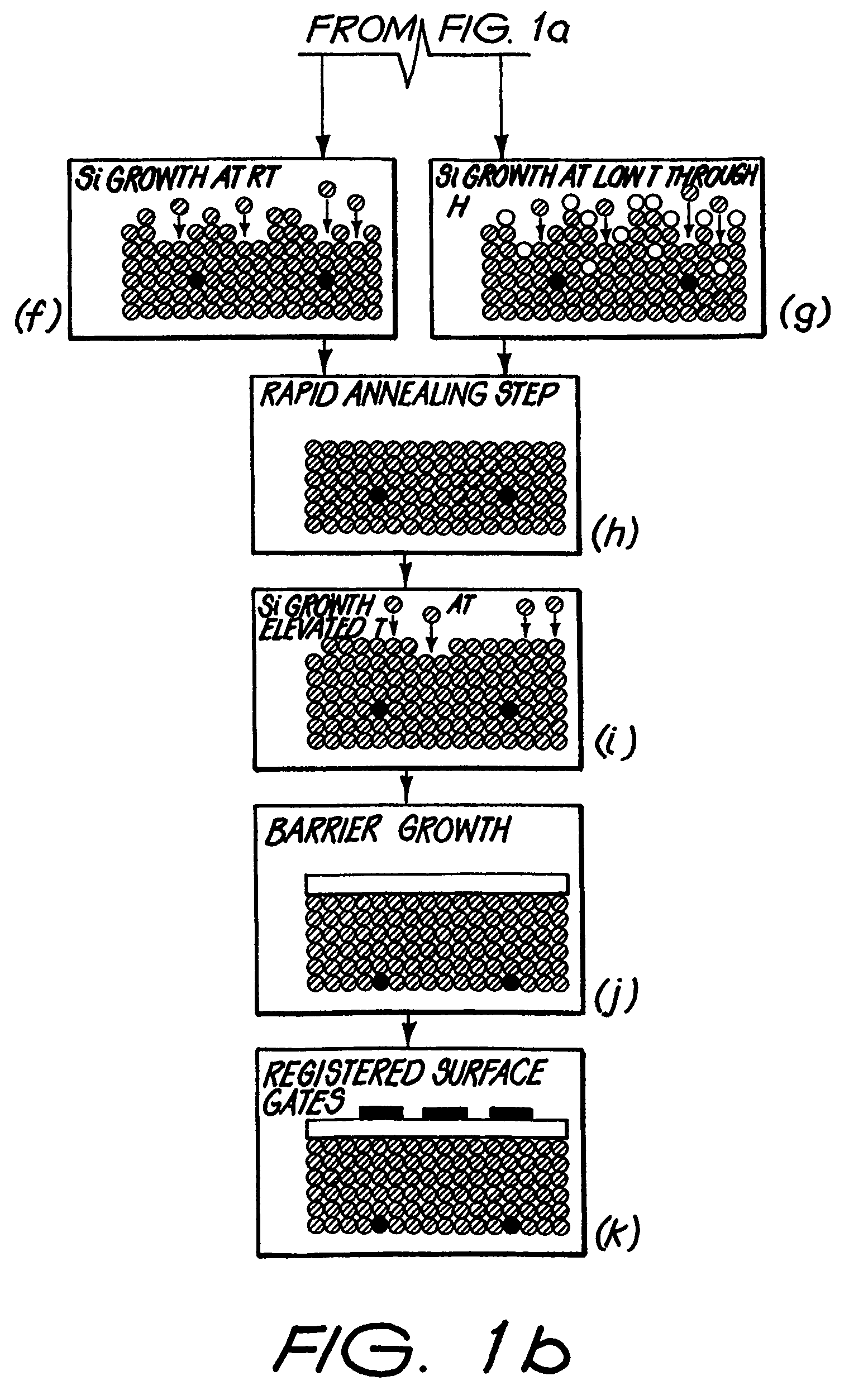
[0102]Referring first to FIGS. 1A and 1B, an outline of the main processing steps of a fabrication strategy for a quantum computing device will be described.

[0103]A clean Si(100)2×1 surface is formed in an ultra-high-vacuum (UHV) by heating to near the melting point. This surface has a 2×1 unit cell and consists of rows of σ-bonded Si dimers with the remaining dangling bond on each Si atom forming a weak π-bond with the other Si atom of the dimer of which it comprises.

[0104]Exposure of this surface to atomic H can break the weak Si π-bonds, allowing H atoms to bond to the Si dangling bonds. Under controlled conditions a monolayer of H can be formed with one H atom bonded to each Si atom, satisfying the reactive dangling bonds, effectively passivating the surface; see FIG. 1A(a).

[0105]A STM tip or SEM is then used to selectively desorb H atoms from the passivated surface by the application of appropriate voltages and tunnelling currents, forming a pattern in t...


PUM


Abstract

This invention concerns the fabrication of nanoscale and atomic scale devices. The method involves creating one or more registration markers. Using a SEM or optical microscope to form an image of the registration markers and the tip of a scanning tunnelling microscope (STM). Using the image to position and reposition the STM tip to pattern the device structure. Forming the active region of the device and then encapsulating it such that one or more of the registration markers are still visible to allow correct positioning of surface electrodes. The method can be used to form any number of device structures including quantum wires, single electron transistors, arrays or gate regions. The method can also be used to produce 3D devices by patterning subsequent layers with the STM and encapsulating in between.

Description

TECHNICAL FIELD [0001]This invention concerns the fabrication of nanoscale and atomic scale devices, that is electronic devices fabricated to nanometer or atomic accuracy. Such devices could be intermediate devices in the fabrication of a quantum computer, but could have many other uses. In a further aspect the invention concerns the devices themselves.BACKGROUND ART [0002]It is known that the Scanning Tunnelling Microscope (STM) can not only image at the atomic scale, but can also be used to manipulate matter at the atomic scale. Research groups are therefore interested in using a STM to fabricate atomic scale semiconductor devices, and very recently it has been shown that it is possible to use a STM to pattern P donors in silicon with atomic precision5.[0003]It is desirable to connect macroscopic leads to a buried nano or atomic-scale patterned conducting region made with a STM once it is removed from the vacuum environment. A difficulty arises when the patterned conducting region...

Claims


Application Information

Patent Timeline
Patent Type & Authority Patents(United States)
IPC IPC(8): H01L21/00B82B1/00B82B3/00H01L21/335H01L23/544
CPCB82Y10/00B82Y30/00G01Q80/00H01L23/544H01L29/66439H01L2223/54453Y10S438/975H01L2924/0002H01L2223/54426H01L2924/00
Inventor RUESS, FRANK J.OBERBECK, LARSSIMMONS, MICHELLE YVONNEGOH, K. E. JOHNSONHAMILTON, ALEXANDER RUDOLFMITIC, MLADENBRENNER, ROLFCURSON, NEIL JONATHANHALLAM, TOBY
Owner NEWSOUTH INNOVATIONS PTY LTD
Why Eureka
Try Eureka