Method and apparatus for power consumption optimization for integrated circuits

a technology of integrated circuits and optimization methods, applied in the direction of instruments, process and machine control, material dimension control, etc., can solve the problems of increasing design verification challenges for such low-power devices, non-battery operated devices of excess heat production, and the need to reduce power not only in battery-operated devices, so as to achieve the effect of meeting timing (slack) requirements and minimizing the power consumption of the entire design

Inactive Publication Date: 2009-06-23
CADENCE DESIGN SYST INC
View PDF16 Cites 30 Cited by
  • Summary
  • Abstract
  • Description
  • Claims
  • Application Information

AI Technical Summary

Benefits of technology

[0010]Hence the goal in one embodiment is to find an assignment of voltages to each power domain in the IC de...

Problems solved by technology

This has resulted in increasing design and verification challenges for such low-power devices.
There is also the corresponding problem in non-battery operated devices of excess heat production given the relatively large amounts of electric power typically used by current integrated circuits.
Hence the need to reduce power is present not only in battery-operated devices but also in devices provided with mains electric current, due to the heat problem.
Such power management issues become more critical in view of the continuous shrinking of integrated circuit (chip) device dimensions, that is the size of transistors, with each subsequent generation of transistors becoming smaller.
Hence more and more power is b...

Method used


Image

  • Method and apparatus for power consumption optimization for integrated circuits
  • Method and apparatus for power consumption optimization for integrated circuits
  • Method and apparatus for power consumption optimization for integrated circuits

Examples


Embodiment Construction

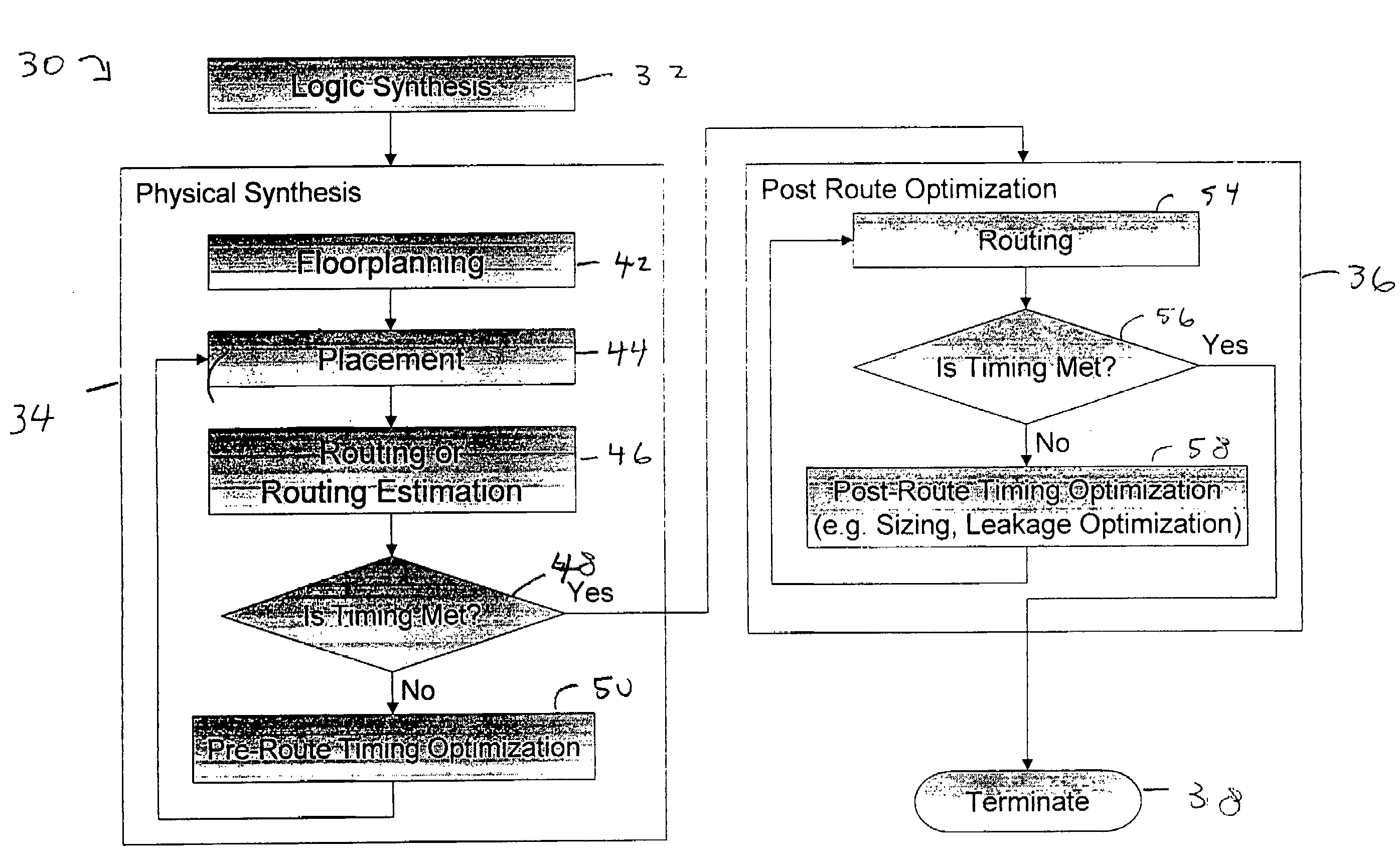
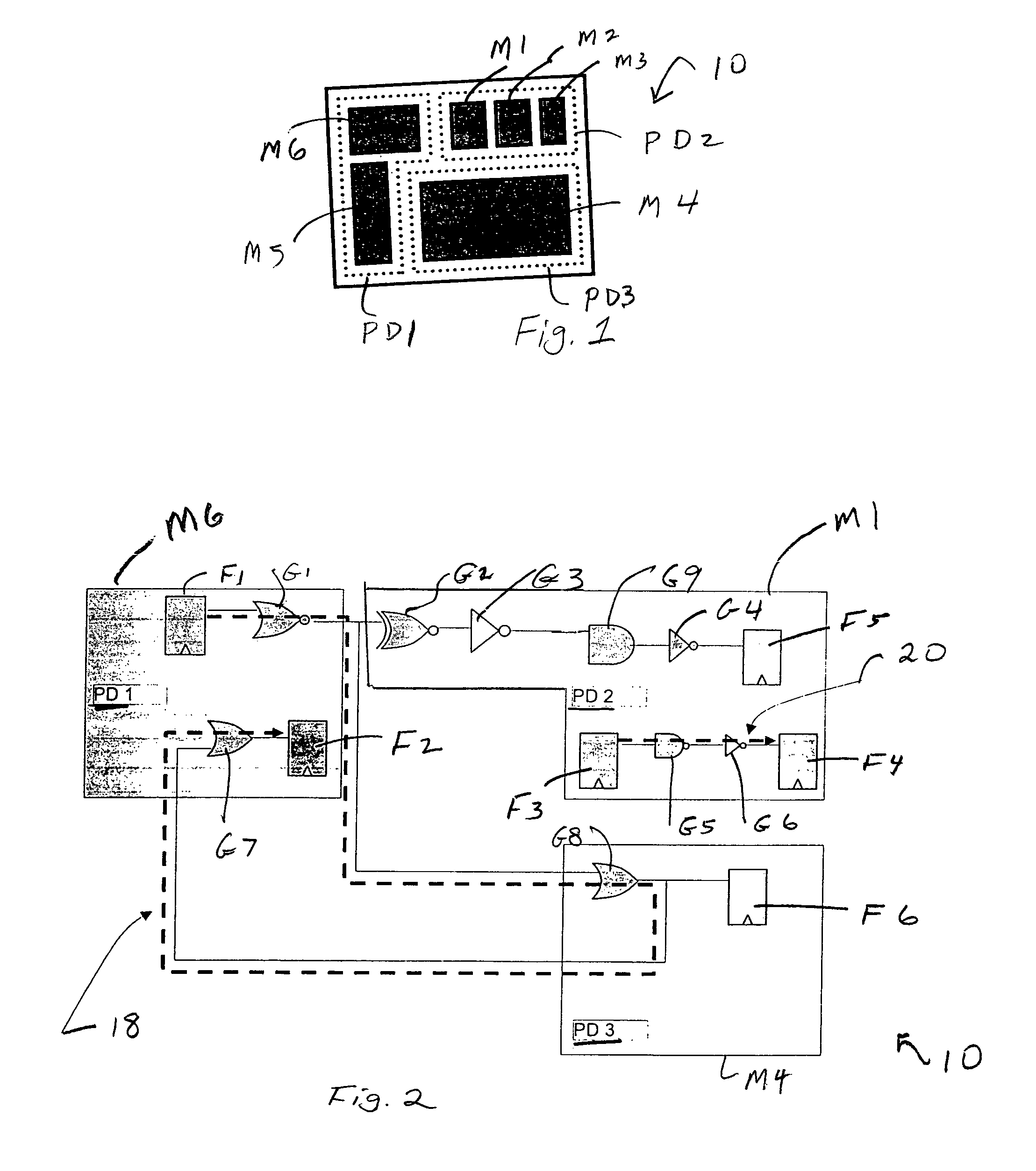
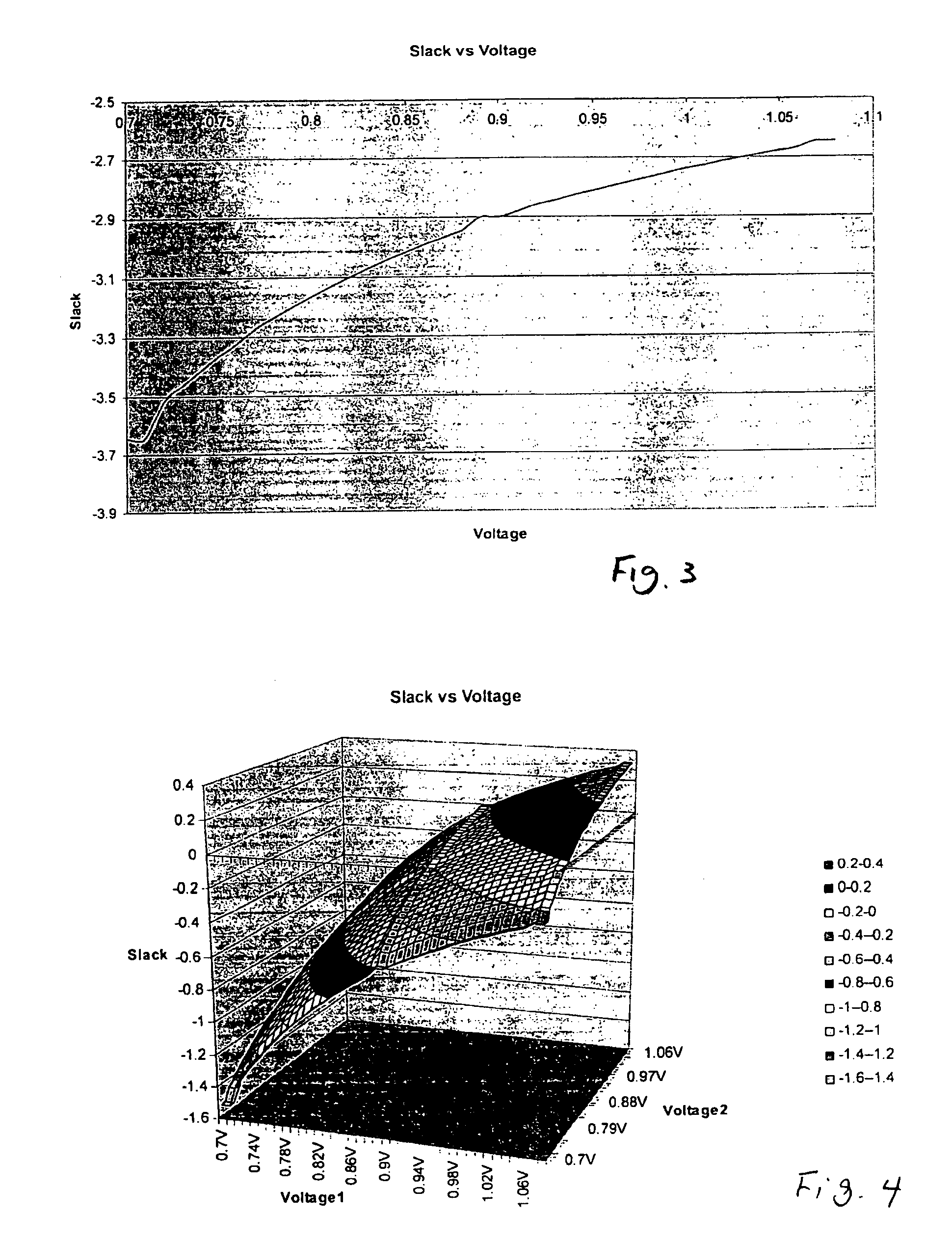
[0027]In one embodiment, this disclosure is directed to a method for simulating and / or designing an integrated circuit having a plurality of power domains, where each power domain has a set of power characteristics (electric power supply characteristics), and is capable of being powered up / powered down independent of other power domains of the circuit and of having a different level of voltage supplied to it compared to other power domains. The present method includes receiving a netlist description of the integrated circuit design in a gate-level representation or equivalent, receiving power information specifications of the circuit design, associating the plurality of power domains in the power information specifications in the netlist description, determining internal and external critical signal paths the circuit design, and assigning a minimum voltage level for each power domain and optimizing (minimizing) the power consumption of the entire circuit design.

[0028]In another embo...


PUM


Abstract

Method and apparatus for finding an assignment of voltages to all power domains of an integrated circuit such that the power consumption of an integrated circuit design is minimized and timing requirements (signal propagation delay or slack) are met. This is done by modeling both internal and external signal paths in an integrated circuit which has a number of power domains. The relationship between slack and voltage for the external and internal signal propagation paths is modeled, typically as a linear approximation. The integrated circuit design is then abstracted to a simplified form in terms of power domain relations and a model is created and solved iteratively using, e.g., linear programming, of different voltage levels for each power domain and including the slack values and their relationship between the changes in voltage and slack, for both the internal and external paths.

Description

FIELD OF THE INVENTION[0001]This disclosure relates to the field of electronic design automation (EDA) tools and to integrated circuit design and simulation.BACKGROUND OF THE INVENTION[0002]With the rapid growth of wireless and portable consumer electronic devices, there have been increasing demands for new technological advancements with more and more functionalities being put into battery-operated electronic devices. This has resulted in increasing design and verification challenges for such low-power devices. There is also the corresponding problem in non-battery operated devices of excess heat production given the relatively large amounts of electric power typically used by current integrated circuits. Hence the need to reduce power is present not only in battery-operated devices but also in devices provided with mains electric current, due to the heat problem.[0003]The pertinent challenges included minimizing leakage power dissipation, designing efficient packaging and cooling ...

Claims


Application Information

Patent Timeline
IPC IPC(8): G06F19/00
CPCG06F17/505G06F2217/78G06F30/327G06F2119/06
Inventor CHEN, PINHONGGOSTI, WILSIN
Owner CADENCE DESIGN SYST INC
Why Eureka
Try Eureka