

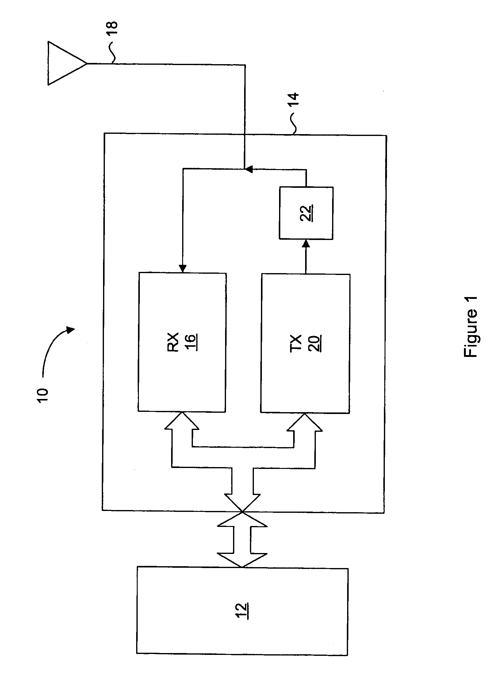
System for reducing second order intermodulation products from differential circuits
a differential circuit and product technology, applied in the field of communication, can solve the problems of prohibitive cost of manufacturing these rf devices, relatively new, complex, and difficult to achieve, and achieve the effect of reducing intermodulation products
- Summary
- Abstract
- Description
- Claims
- Application Information
AI Technical Summary
Benefits of technology
Problems solved by technology
Method used
Image

Examples
Embodiment Construction
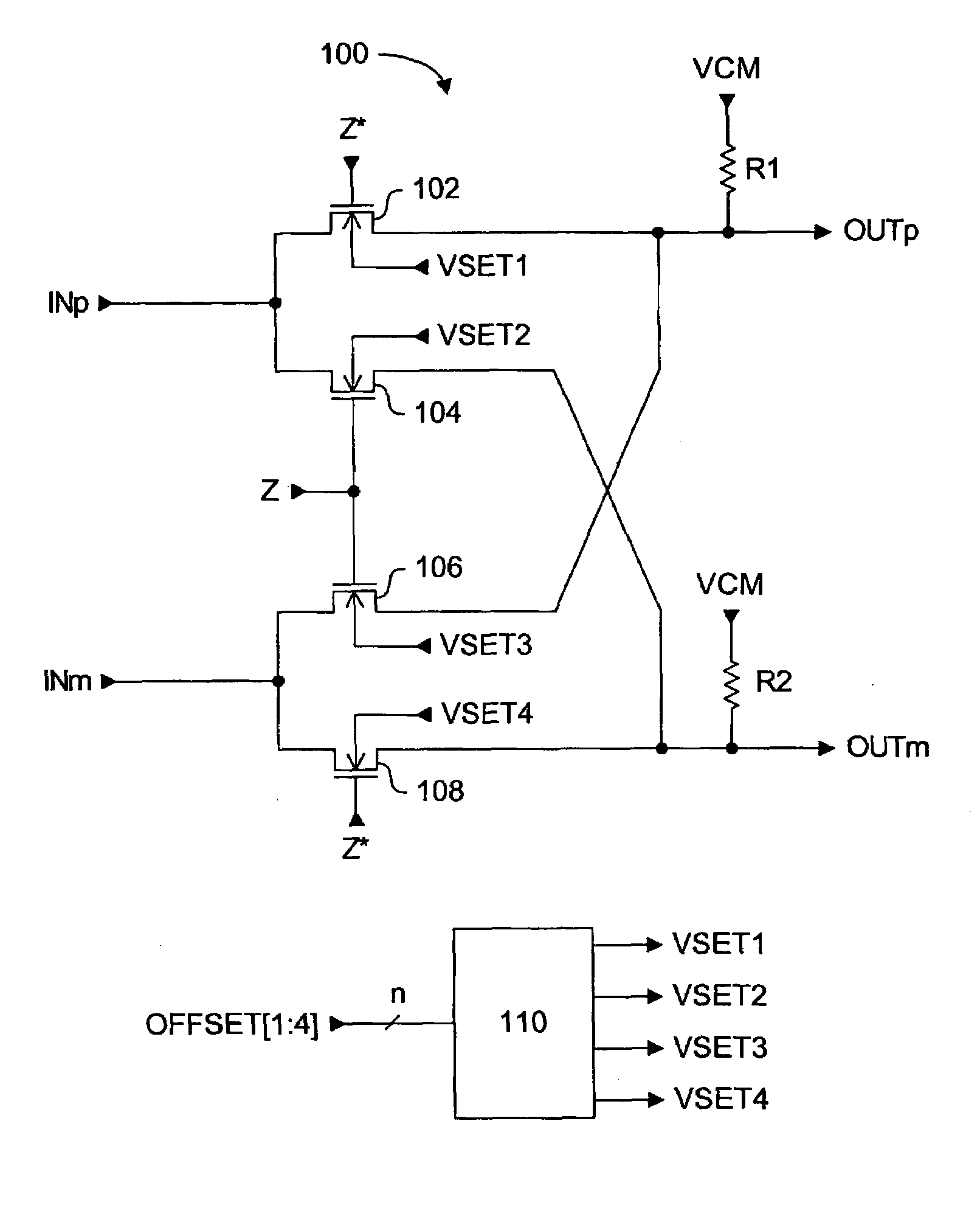
[0044]Generally, the present invention provides a passive CMOS differential mixer circuit with a mismatch correction circuit for balancing the electrical characteristics of the two output paths. Once the output paths of the differential circuit are balanced, or matched as closely as possible, second order intermodulation product generation can be inhibited or at least reduced to acceptable levels. The mismatch correction circuit receives at least one n-bit digital offset signal, to generate one or more corresponding voltages. The generated voltages are applied to the differential mixer circuit to balance its electrical characteristics.
[0045]According to embodiments of the present invention, the voltage signals can be applied to the back gate bias voltages of selected transistors of the circuit to adjust their threshold voltages such that they all match. Alternately, the voltage signals can adjust common mode voltages applied directly to a selected signal path to ensure that their el...
PUM
 Abstract
Description
Claims
Application Information