Test assembly including a test die for testing a semiconductor product die

a technology for testing assembly and product die, which is applied in the direction of semiconductor/solid-state device testing/measurement, semiconductor/solid-state device details, instruments, etc., can solve the problems of increasing and increasing the complexity and density of the integrated circuit design, so as to reduce the effect of reducing the size of the product die and high degree of fault coverag

Inactive Publication Date: 2009-07-07
FORMFACTOR INC
View PDF65 Cites 22 Cited by
  • Summary
  • Abstract
  • Description
  • Claims
  • Application Information

AI Technical Summary

Benefits of technology

[0013]One embodiment of the present invention concerns a test assembly for testing product circuitry of a product die. In one embodiment, the test assembly includes at test die and an interconnection substrate for electrically coupling the test die to a host controller that communicates with the test die. The test die may be designed according to a design methodology that includes the step of concurrently designing test circuitry and a product circuitry in a unified design. The test circuitry can be designed to provide a high degree of fault coverage for the corresponding product circuitry generally without regard to the amount of silicon area that will be required by the test circuitry. The design methodology then partitions the unified design into the test die and the product die. The test die includes the test circuitry and the product die includes the product circuitry. The product and test die may then be fabricated on separate semiconductor wafers. By partitioning the product circuitry and test circuitry into separate die, embedded test circuitry can be either eliminated or minimized on the product die. This will tend to decrease the size of the product die and decrease the cost of manufacturing the product die while maintaining a high degree of test coverage of the product circuits within the product die. The test die can be used to test multiple product die on one or more wafers.

Problems solved by technology

As integrated circuit designs continue to increase in both complexity and density, design methodologies are challenged to create circuits that use Design-For-Test (DFT) techniques to improve the testability and the quality of the final product.
Test methodologies are also challenged to create high-quality, low cost test solutions.
As integrated circuit designs become more complex and operate at higher speeds, they place more demands on the testing equipment.
This tends to increase the cost of ATEs and, thus, tends to increase manufacturing costs.
Additionally, as integrated circuit designs become more complex, the time required to test the circuits increases.
This also tends to increase manufacturing costs.
If a die already has all of its peripheral, grid, or lead-on-center bond pad locations dedicated to a device function, then adding additional bond pads in the predetermined bond pad alignment to support the on-chip testing circuitry can result in a substantial increase in the size of the die.
This tends to have a corresponding increase in the cost of the die.
Generally, larger die are more prone to defects and consequently more expensive to manufacture.
Additionally, on-chip testing circuitry can result in a significant increase in test time as many clock cycles may be required to load test input data and subsequently output test results from a few available bond pads.
On-chip testing circuitry also does not allow for direct external access to internal circuit nodes.
This introduces additional circuits that can mask failures in the circuit intended to be tested, or can introduce new failures caused by SCAN or BIST circuitry.
Additionally, many designs are I / O limited since only a limited number of leads (e.g., bond wires) may be accommodated in a given packaging scheme.
The amount of embedded test circuitry to add to a particular design typically requires balancing the benefits of increased fault coverage and potentially decreased test time (e.g., as compared with an ATE) with the disadvantages of increasing both the die size and probability of fabrication defects which each result in increased manufacturing cost of the end product.
At one extreme, designs could include elaborate embedded test circuits that test every circuit node of all internal circuits, however, these designs would be prohibitively expensive as the die size would primarily be a function of the size of the test circuitry.
This latter approach, however, tends to provide reduced fault coverage, a lower product quality, and increase manufacturing costs by using expensive ATEs and by increasing test times. One approach to minimize the cost of using expensive ATEs is disclosed in U.S. Pat. No. 5,497,079 (the '079 patent).
This balance, however, results in less than optimal fault coverage while still requiring the use of expensive ATEs.

Method used


Image

  • Test assembly including a test die for testing a semiconductor product die
  • Test assembly including a test die for testing a semiconductor product die
  • Test assembly including a test die for testing a semiconductor product die

Examples


Embodiment Construction

[0065]In the following detailed description of the present invention numerous specific details are set forth in order to provide a thorough understanding of the present invention. However, one skilled in the art may practice the invention without these specific details. In some instances, well known methods, procedures, and components have not been described to avoid obscuring the present invention.

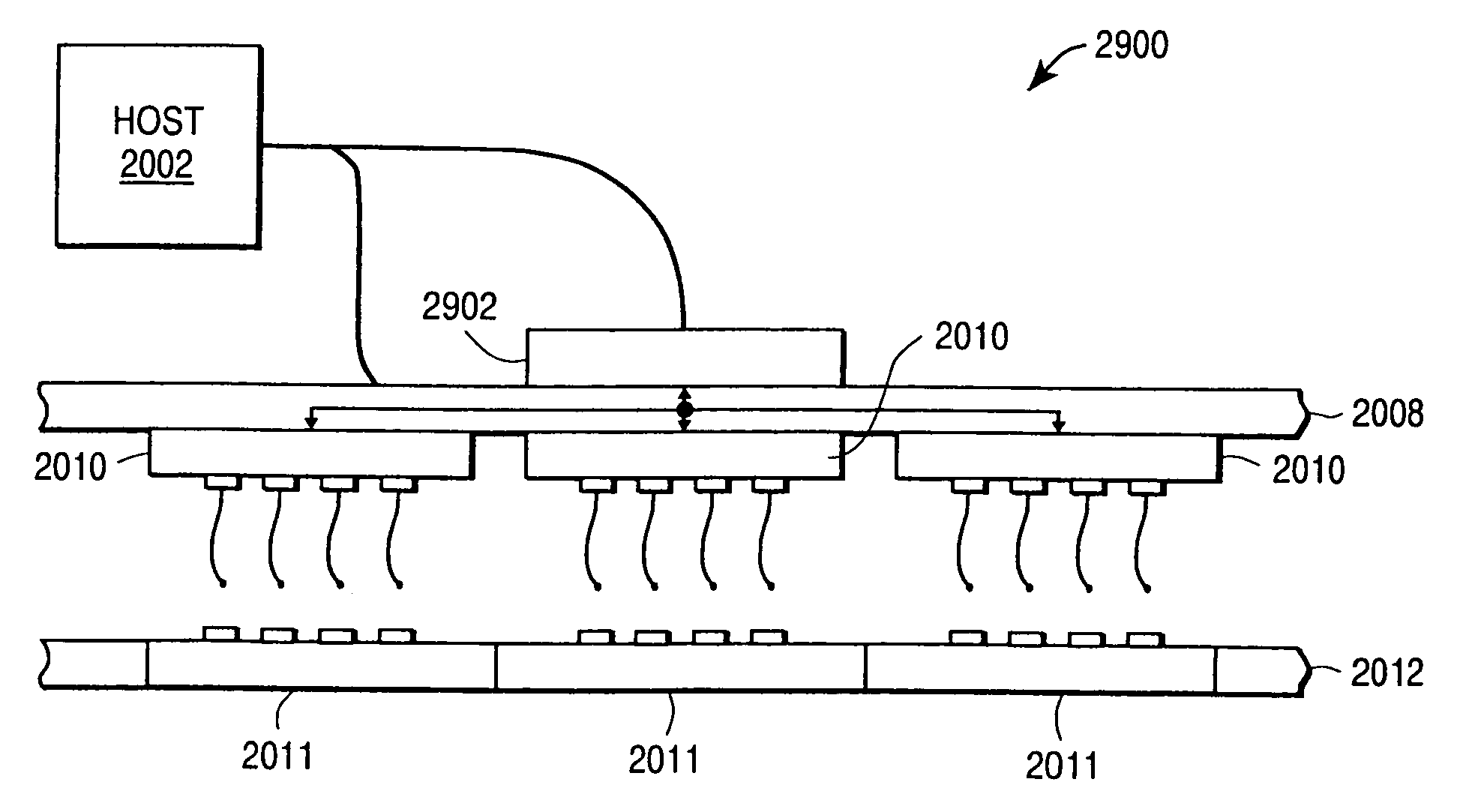
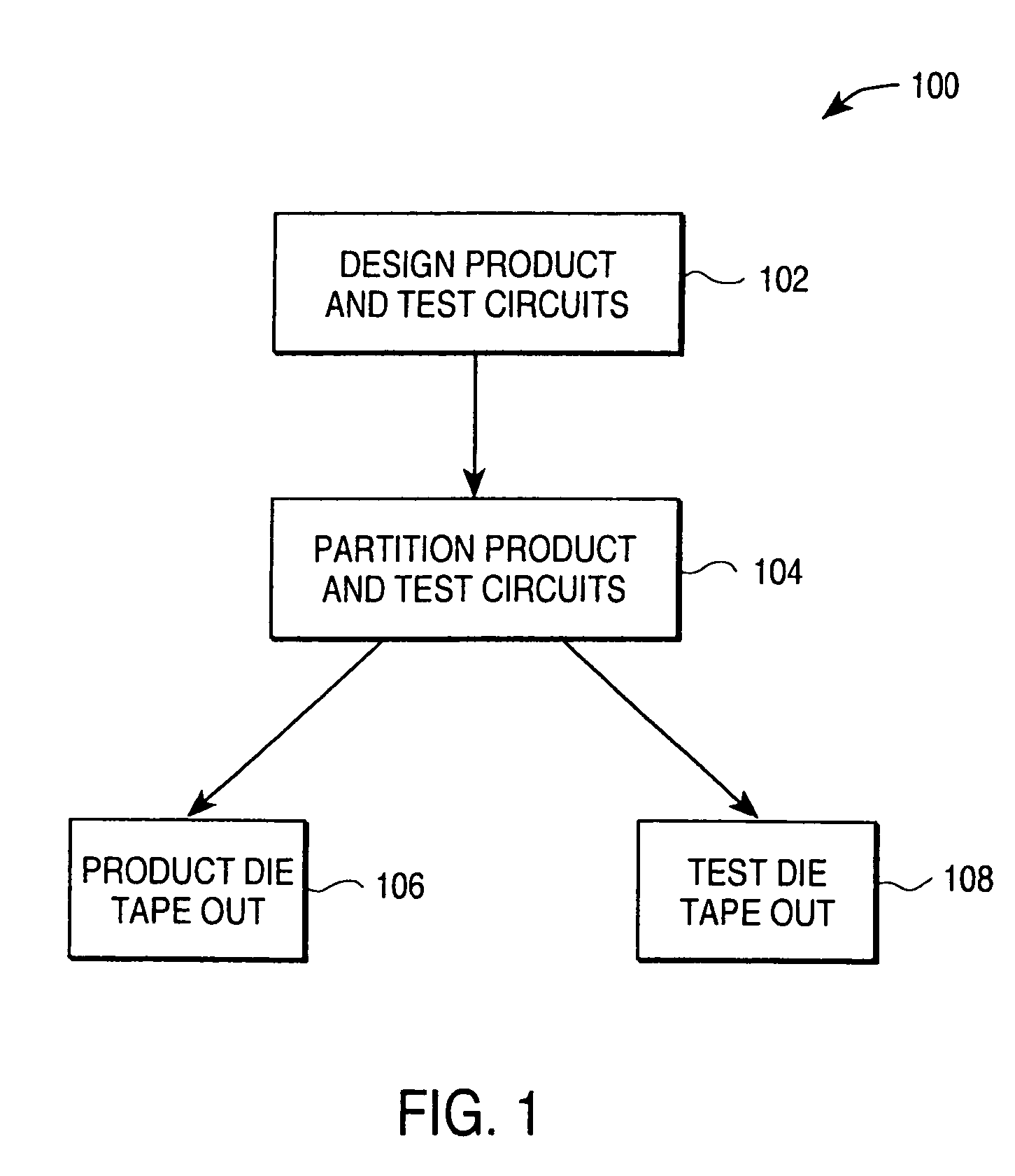
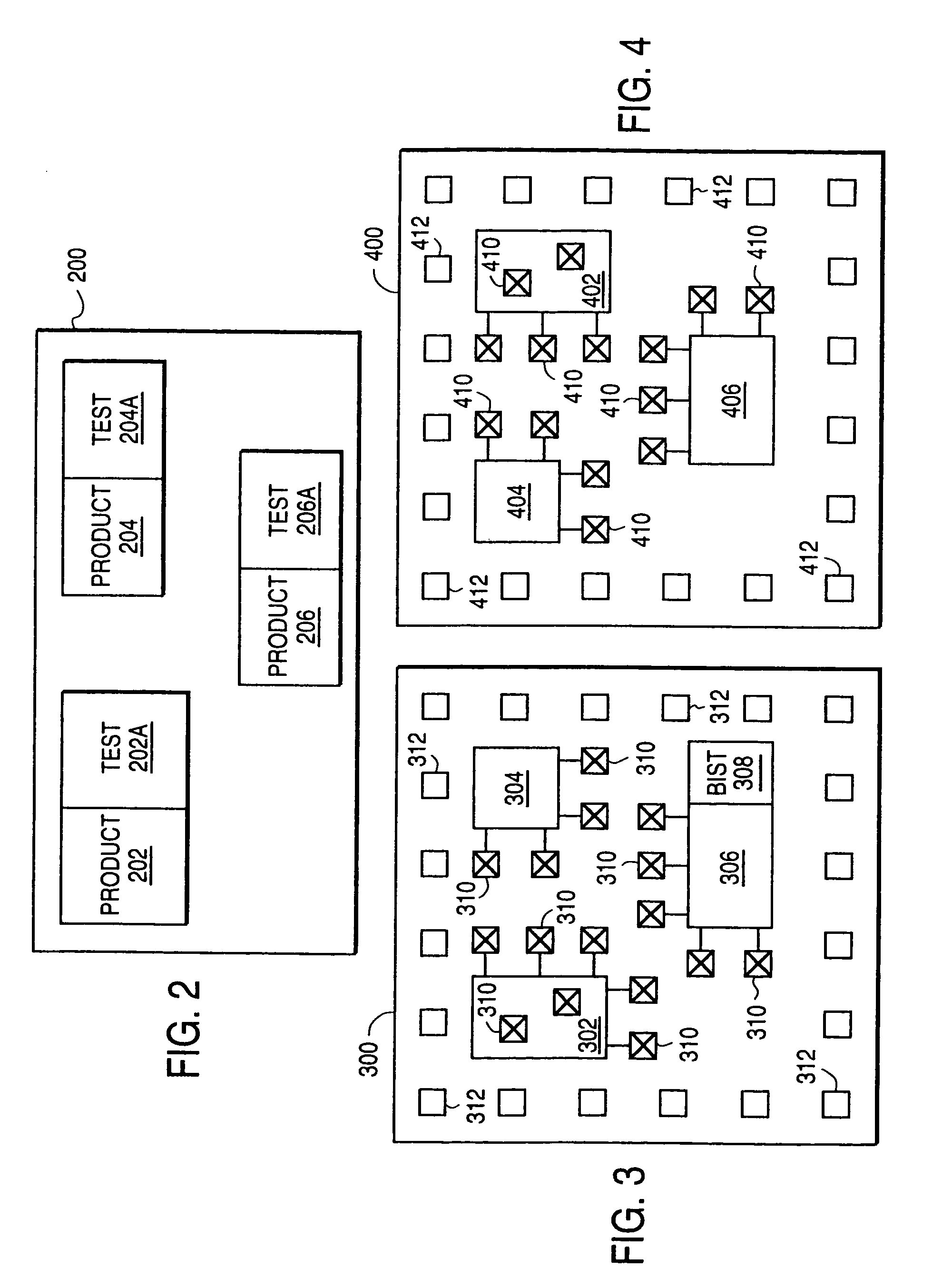
[0066]FIG. 1 shows one embodiment of a design methodology 100 for designing a product die and a corresponding test die that includes test circuitry for providing test signals to, or monitoring signals from, one or more circuits on the product die. FIGS. 2-4 illustrate product die and test die generated by design methodology 100.

[0067]Throughout this application the terms “product die” and “product device” refer to a single instance of an integrated circuit that is formed on a semiconductor wafer or on an insulating or other appropriate substrate. These terms may also refer to a device und...


PUM


Abstract

One embodiment of the present invention concerns a test assembly for testing product circuitry of a product die. In one embodiment, the test assembly includes at test die and an interconnection substrate for electrically coupling the test die to a host controller that communicates with the test die. The test die may be designed according to a design methodology that includes the step of concurrently designing test circuitry and a product circuitry in a unified design. The test circuitry can be designed to provide a high degree of fault coverage for the corresponding product circuitry generally without regard to the amount of silicon area that will be required by the test circuitry. The design methodology then partitions the unified design into the test die and the product die. The test die includes the test circuitry and the product die includes the product circuitry. The product and test die may then be fabricated on separate semiconductor wafers. By partitioning the product circuitry and test circuitry into separate die, embedded test circuitry can be either eliminated or minimized on the product die. This will tend to decrease the size of the product die and decrease the cost of manufacturing the product die while maintaining a high degree of test coverage of the product circuits within the product die. The test die can be used to test multiple product die on one or more wafers.

Description

CROSS-REFERENCE TO RELATED APPLICATIONS[0001]This patent application is a continuation-in-part application of commonly-owned, co-pending U.S. patent application Ser. No. 08 / 784,862 filed Jan. 15, 1997 which is incorporated by reference herein, and from which priority is claimed.FIELD OF THE INVENTION[0002]The present invention relates to integrated circuit (IC) semiconductor devices and, more particularly, to testing the devices.BACKGROUND[0003]As integrated circuit designs continue to increase in both complexity and density, design methodologies are challenged to create circuits that use Design-For-Test (DFT) techniques to improve the testability and the quality of the final product. Test methodologies are also challenged to create high-quality, low cost test solutions.[0004]One conventional design methodology includes the process of initially designing an integrated circuit using a software design tool, simulating the overall functionality of the design or individual circuits with...

Claims


Application Information

Patent Timeline
Patent Type & Authority Patents(United States)
IPC IPC(8): G01R31/02G01R1/067G01R1/073G01R31/28H01L23/48H01L23/485H01L23/498H01L23/544H05K3/20H05K3/34
CPCG01R1/07307G01R1/07342H01L24/13G01R1/07371G01R31/2884H01L22/34H01L23/49811H01L24/06H01L24/10H01L24/72H01L2224/0401H01L22/32H01L2924/10253H01L2924/01076H01L2924/01033H01L2924/01023H01L2924/01005H05K3/3421G01R31/2886H01L2224/04042H01L2224/05553H01L2224/05624H01L2224/05644H01L2224/05647H01L2224/06136H01L2224/13099H01L2924/01006H01L2924/01013H01L2924/01014H01L2924/01027H01L2924/01029H01L2924/01074H01L2924/01079H01L2924/01082H01L2924/014H01L2924/14H01L2924/19041H01L2924/19043H05K3/20H01L2924/00014H01L2924/00H01L24/05H01L2224/13H01L2924/12042
Inventor ELDRIDGE, BENJAMIN N.KHANDROS, IGOR Y.PEDERSEN, DAVID V.WHITTEN, RALPH G.
Owner FORMFACTOR INC
Why Eureka
Try Eureka