Hybrid capacitor

a hybrid capacitor and capacitor technology, applied in the manufacture of electrolytic capacitors, semiconductor/solid-state devices, fixed capacitor details, etc., can solve the problems of difficult removal of high-frequency noise, increased parasitic inductance, and insufficient arrangement of smd capacitors on circuit boards, etc., to achieve stable voltage, remove high-frequency interference, and large capacitance

Active Publication Date: 2009-07-14
IND TECH RES INST
View PDF12 Cites 21 Cited by
  • Summary
  • Abstract
  • Description
  • Claims
  • Application Information

AI Technical Summary

Benefits of technology

[0007]The present invention is directed to a hybrid capacitor capable of providing large capacitance so as to stabilize voltage between chips and remove high-frequency interference.
[0009]In the present invention, the through hole capacitor having the anode layer with the porous structure is connected in parallel with the plate capacitor, and thus a hybrid capacitor having large capacitance is obtained. Moreover, the hybrid capacitor of the present invention capable of fulfilling the requirements is designed through coordinating the through hole capacitors having the anode layer with the porous structure and the plate capacitors. Hence, the hybrid capacitor of the present invention provides a capacitance larger than 0.1 μF within the size of a chip to stabilize voltage among chips and simultaneously remove high-frequency interference of 1-4 GHz.

Problems solved by technology

As a number of stacked layers increases, arranging SMD capacitors on a circuit board is not sufficient to fulfill the requirement of stabilizing a common voltage when a plurality of layers of chips are stacked together.
Furthermore, as the working frequency of ICs increases, if high frequency noise is removed only by a decoupling capacitor on the circuit board, since a transmission path is too long because of stacking multiple layers of ICs, parasitic inductance are therefore increased and high frequency noise would be difficult to remove.

Method used


Image

  • Hybrid capacitor
  • Hybrid capacitor
  • Hybrid capacitor

Examples


first embodiment

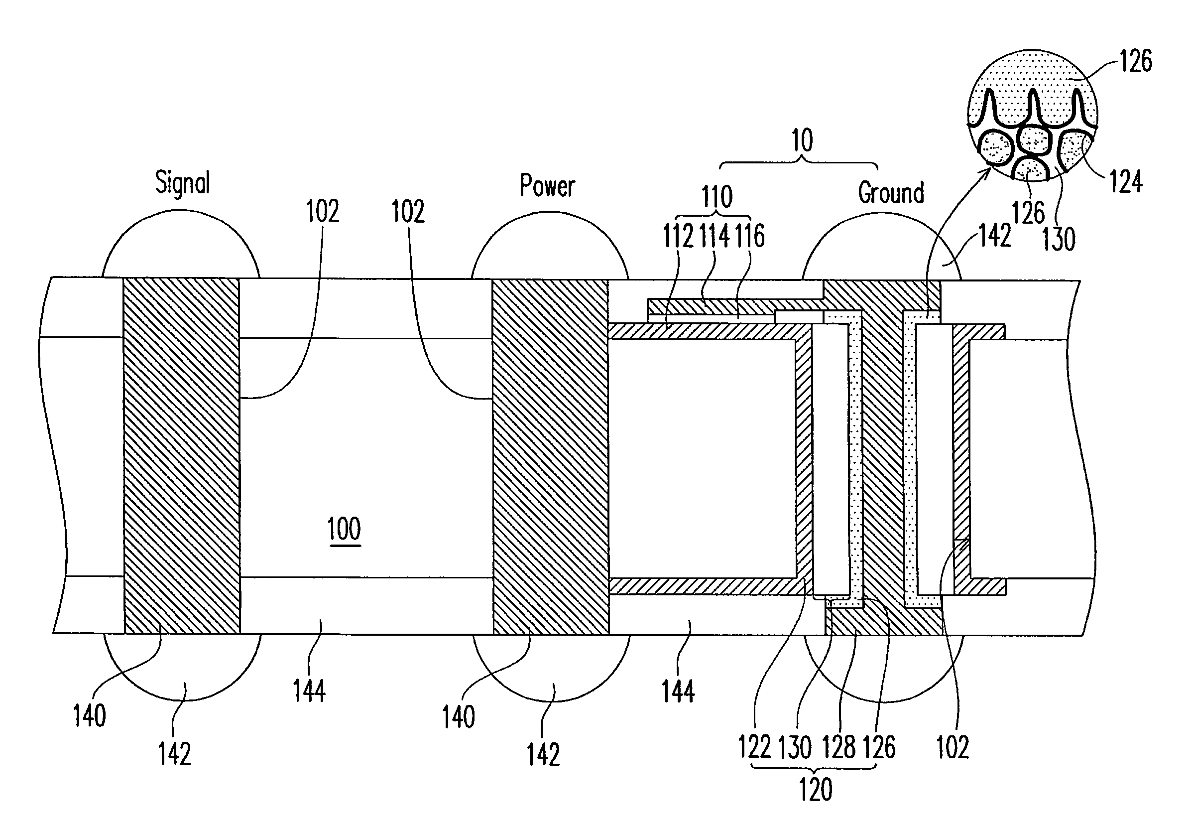
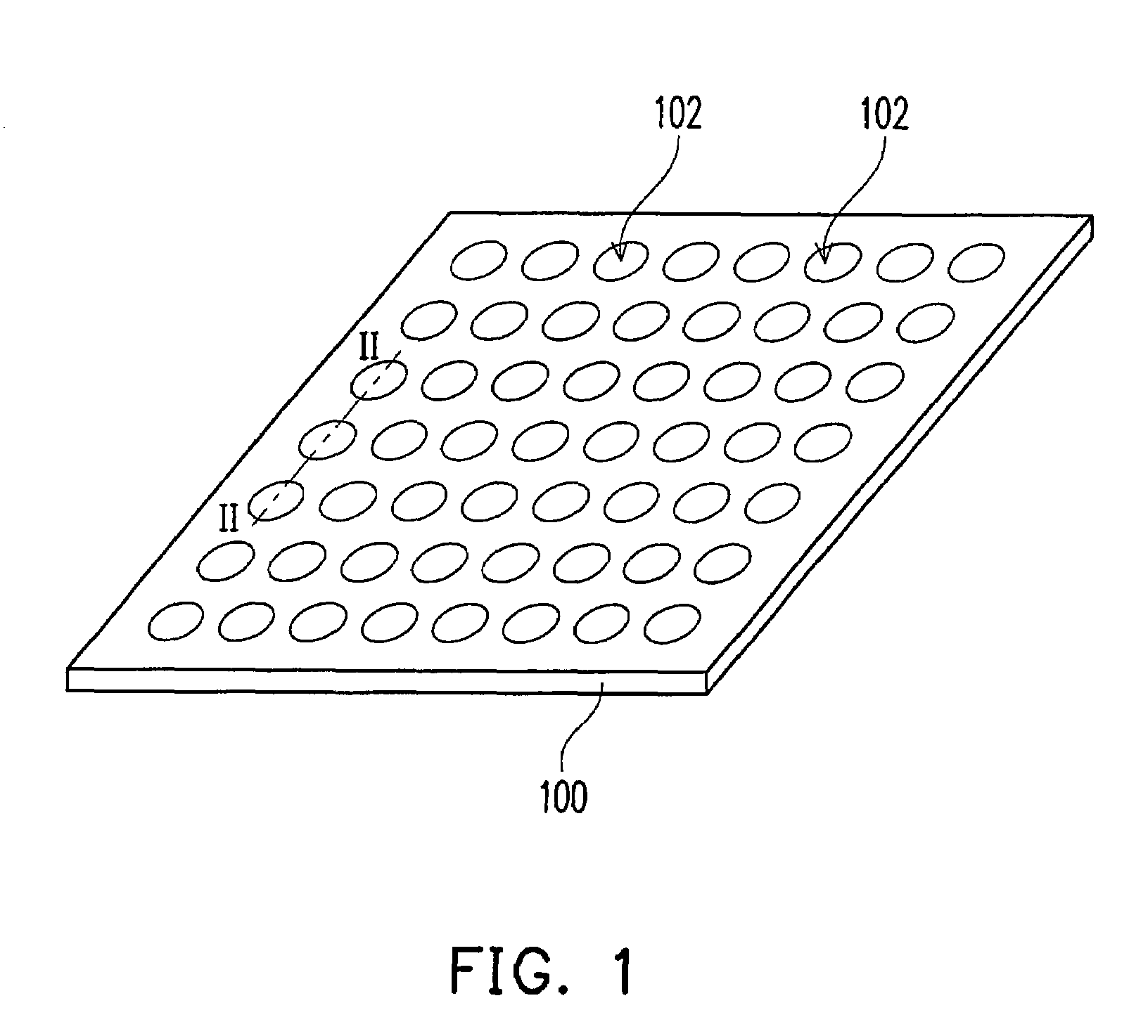
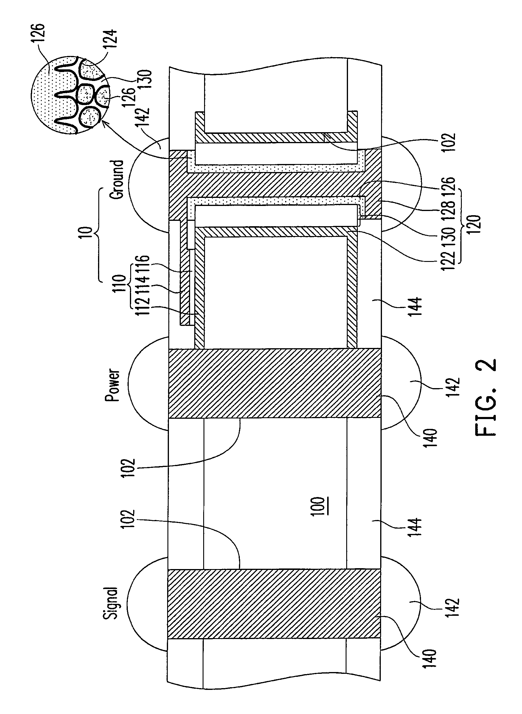
[0022]FIG. 1 is a substrate having a hybrid capacitor or a silicon interposer according to the present invention. FIG. 2 is a schematic cross-sectional view along line II-II of FIG. 1.

[0023]Referring to FIGS. 1 and 2, a hybrid capacitor 10 of the first embodiment includes a substrate 100, at least one plate capacitor 110 and at least one through hole capacitor 120. The substrate 100 has a plurality of through holes 102 and the plate capacitor 110 is disposed on the substrate 100. The through hole capacitors 120 are disposed in at least one through hole 102 and connected in parallel with the plate capacitor 110. The through hole capacitor 120 at least includes an anode layer 122, a first dielectric layer 124, a first cathode layer 126 and a second cathode layer 128. According to the first embodiment of the present invention, the substrate 100 is a silicon substrate. The substrate 100 may also be an organic substrate, a metal substrate or an insulating substrate. The through holes 102...

second embodiment

[0029]FIG. 4 is a schematic cross-sectional view of a hybrid capacitor according to the present invention.

[0030]Referring to FIG. 4, a hybrid capacitor 40 of the second embodiment includes a metal substrate 400, at least one plate capacitor 410 and at least one through hole capacitor 420. The metal substrate 400 has a plurality of through holes 402. A portion of the metal substrate 400 can serve as a first conductive layer 412 of the plate capacitor 410. A second conductive layer 414 of the plate capacitor 410 is disposed on a surface of a second dielectric layer 416. The second dielectric layer 416 is disposed between the metal substrate 400 and the second conductive layer 414. For materials which may be selected to fabricate the second dielectric layer 416, please refer to those materials previously listed in the first embodiment.

[0031]Referring to FIG. 4, the through hole capacitor 420 is disposed in the through hole 402 and is connected in parallel with the plate capacitor 410. ...

third embodiment

[0032]FIG. 5 is a top view of a hybrid capacitor according to the present invention. FIG. 6 is a schematic cross-sectional view along line VI-VI of FIG. 5.

[0033]Referring to FIGS. 5 and 6, a hybrid capacitor 50 of the third embodiment includes a substrate 500, at least one plate capacitor 510 and at least one through hole capacitor 520. The substrate 500 has a through hole 502 and the through hole capacitor 520 is disposed in the through hole 502. A structure of the through hole capacitor 520 is identical to that of the through hole capacitor in the first embodiment, and therefore the reference numerals of the first embodiment are adopted herein to represent the same or similar elements. The plate capacitor 510 is disposed on the substrate 500 surrounding the through hole capacitor 520 and connected in parallel therewith. A structure of the plate capacitor 510 is identical to that of the plate capacitor in the first embodiment, and therefore the reference numerals of the first embod...


PUM


Abstract

A hybrid capacitor is provided which includes a substrate, at least one plate capacitor and at least one through hole capacitor. The substrate has through holes and the plate capacitors are on the substrate. At least one through hole capacitor and at least one plate capacitor are in parallel. The through hole capacitor at least includes an anode layer, a first dielectric layer, a first cathode layer and a second cathode layer. The anode layer is disposed on an inner surface of at least one through hole, and a surface of the anode layer is a porous structure. The first dielectric layer is disposed on the porous structure of the anode layer and covered with the first cathode layer. The first cathode layer is covered with the second cathode layer. A conductivity of the second cathode layer is larger than a conductivity of the first cathode layer.

Description

CROSS-REFERENCE TO RELATED APPLICATION[0001]This application claims the priority benefit of Taiwan application serial no. 96149241, filed on Dec. 21, 2007. The entirety the above-mentioned patent application is hereby incorporated by reference herein and made a part of specification.BACKGROUND OF THE INVENTION[0002]1. Field of the Invention[0003]The present invention is related to a hybrid capacitor capable of stabilizing a voltage and reducing noise on a high frequency and a method of fabricating the same.[0004]2. Description of Related Art[0005]In order to meet the demand for multiple functions in electronic products, the latest trend in the system in package (SiP) technology tends to package integrated circuits (IC) having different functions into one multi-functional IC module in a three-dimensional stacking mode. When different ICs are integrated by three-dimensional stacking, in order to solve the problem of mismatch between the upper and lower layers of IC pins, an interposer...

Claims


Application Information

Patent Timeline
Patent Type & Authority Patents(United States)
IPC IPC(8): H01G9/025
CPCH01G9/0029H01G9/012H01G9/15H01L23/642H01L28/40H01L2924/12044H01L2924/0002H01L2924/19015H01L2924/3011H01L2924/00Y02E60/13H01L23/481
Inventor LEE, MIN-LINTSAI, LI-DUANLIU, SHUR-FENWU, BANG-HAOCHENG, CHENG-LIANG
Owner IND TECH RES INST
Why Eureka
Try Eureka