Method of fabricating poly-crystalline silicon thin film and method of fabricating transistor using the same

a technology of polysi and thin film, which is applied in the direction of transistors, chemical vapor deposition coatings, coatings, etc., can solve the problem that polysi tft must be fabricated, and achieve the effect of increasing energy and increasing si grain siz

Inactive Publication Date: 2009-07-21
SAMSUNG ELECTRONICS CO LTD
View PDF1 Cites 205 Cited by
  • Summary
  • Abstract
  • Description
  • Claims
  • Application Information

AI Technical Summary

Benefits of technology

[0015]The diluted He may be an He / SiH4 composition and a ratio of He to SiH4 may be in a range from 6 to 12, preferably 10, that is, 20:2. A deposition ratio of silicon by the ICP-CVD may be 2.8 Å / sec. The poly-Si can be annealed using ELA, thereby increasing Si grain size. The ELA is performed while increasing energy by predetermined steps.

Problems solved by technology

However, such a poly-Si TFT must be fabricated at a low temperature because a plastic substrate is heat intolerant.

Method used


Image

  • Method of fabricating poly-crystalline silicon thin film and method of fabricating transistor using the same
  • Method of fabricating poly-crystalline silicon thin film and method of fabricating transistor using the same
  • Method of fabricating poly-crystalline silicon thin film and method of fabricating transistor using the same

Examples


Embodiment Construction

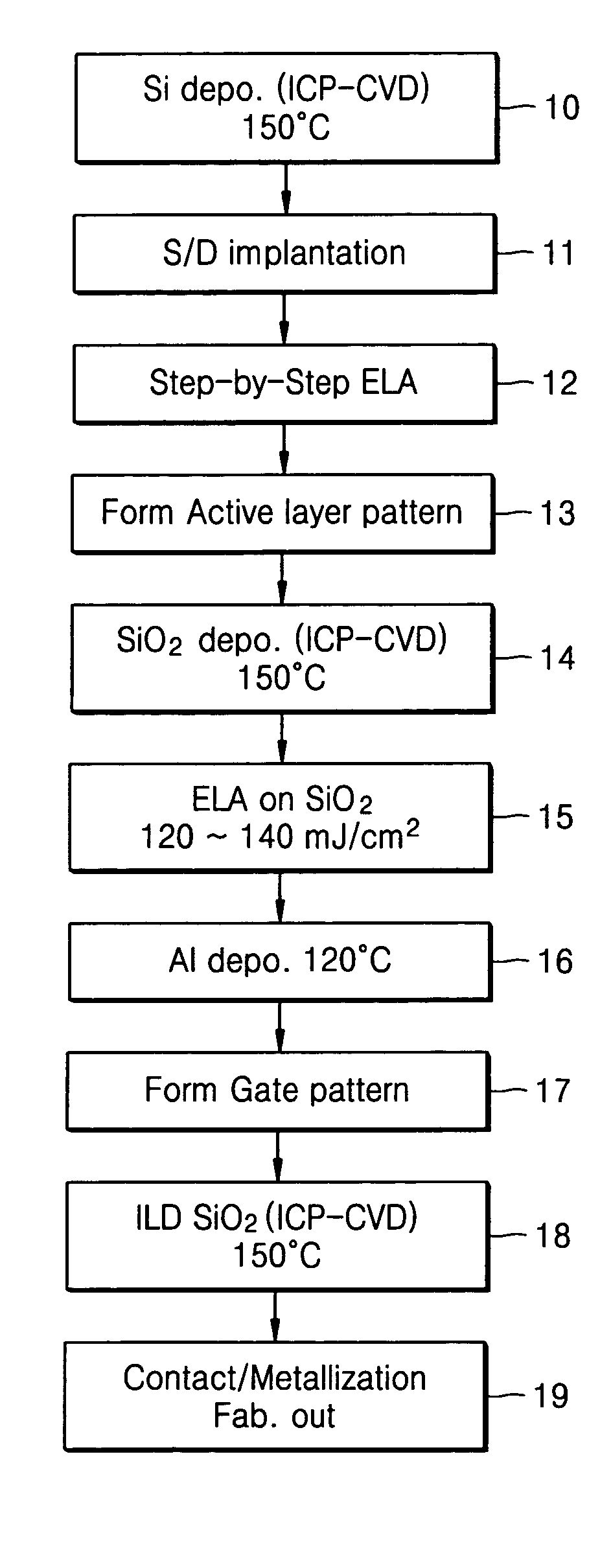
[0029]Hereinafter, a method of fabricating a poly-Si thin film and a method of fabricating a TFT using the same according to the present disclosure will be described in detail with reference to the accompanying drawings.

[0030]1. Deposition of Silicon Thin Film

[0031]High density plasma generated by inductively coupled plasma chemical vapor deposition (ICP-CVD) has a high deposition ratio. ICP-CVD uses remote plasma, which can reduce ion damage in a film-growth zone.

[0032]An active layer of a poly-Si TFT is formed by the ICP-CVD. At this time, He / SiH4 gas diluted with He can be used. Also, a substrate temperature of 150° C. and a pressure of 22 mTorr are maintained. A ratio of He to SiH4 is 10, that is, 20:2 [sccm], and a deposition rate is 2.8 Å / sec.

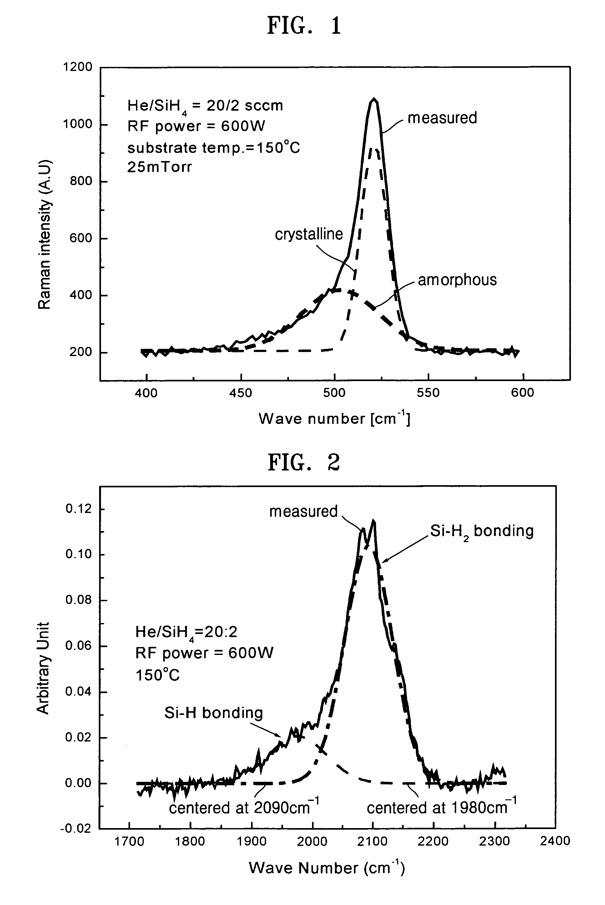
[0033]FIG. 1 is a graph illustrating a Raman spectrum of a deposited silicon film. Referring to FIG. 1, it can be seen that the silicon film has a crystal structure, as indicated by a dominant peak of 520 cm−1. An amorphous / intermediate p...


PUM

PropertyMeasurementUnit
pressureaaaaaaaaaa
temperatureaaaaaaaaaa
flat-band voltageaaaaaaaaaa

Abstract

A method of fabricating a poly-Si thin film and a method of fabricating a poly-Si TFT using the same are provided. The poly-Si thin film is formed at a low temperature using inductively coupled plasma chemical vapor deposition (ICP-CVD). After the ICP-CVD, excimer laser annealing (ELA) is performed while increasing energy by predetermined steps. A poly-Si active layer and a SiO2 gate insulating layer are deposited at a temperature of about 150° C. using ICP-CVD. The poly-Si has a large grain size of about 3000 Å or more. An interface trap density of the SiO2 can be as high as 1011 / cm2. A transistor having good electrical characteristics can be fabricated at a low temperature and thus can be formed on a heat tolerant plastic substrate.

Description

BACKGROUND OF THE DISCLOSURE[0001]This application claims the priority of Korean Patent Application No. 2003-88423, filed on Dec. 6, 2003, in the Korean Intellectual Property Office, the disclosure of which is incorporated herein in its entirety by reference.[0002]1. Field of the Disclosure[0003]The present disclosure relates to a method of fabricating poly-Si thin film and a method of fabricating a transistor using the same, and more particularly, to a method of fabricating a poly-Si thin film having high mobility and a method of fabricating a transistor using the same.[0004]2. Description of the Related Art[0005]Poly-crystalline silicon (poly-Si) is applied to a variety of electronic devices such as flat panel displays and solar cells because it has greater mobility than amorphous silicon (a-Si). Generally, poly-Si electronic devices are formed on a substrate of a heat resistant material, such as glass. A method of fabricating a poly-Si electronic device on a plastic substrate has...

Claims


Application Information

Patent Timeline
Patent Type & Authority Patents(United States)
IPC IPC(8): H01L21/00H01L21/205C23C16/24H01L21/20H01L21/316H01L21/336H01L29/49H01L29/786
CPCH01L21/02164H01L21/02274H01L21/02354H01L29/78675H01L21/31608H01L29/4908H01L29/66757H01L21/2026H01L21/0262H01L21/02686H01L21/02422H01L21/02532H01L29/786H01L21/02595
Inventor KWON, JANG-YEONHAN, MIN-KOOCHO, SE-YOUNGPARK, KYUNG-BAEKIM, DO-YOUNGLEE, MIN-CHEOLHAN, SANG-MYEONNOGUCHI, TAKASHIPARK, YOUNG-SOOJUNG, JI-SIM
Owner SAMSUNG ELECTRONICS CO LTD
Why Eureka
Try Eureka