Variable sized aperture window of an analog-to-digital converter

an analog-to-digital converter and variable-sized aperture technology, applied in the field of computer processors, can solve the problems of not allowing embedding, requiring more expensive chips, and only possible reproduction, and achieve the effect of faster sampling ra

Inactive Publication Date: 2009-08-11
ARRAY PORTFOLIO
View PDF14 Cites 1 Cited by
  • Summary
  • Abstract
  • Description
  • Claims
  • Application Information

AI Technical Summary

Benefits of technology

[0023]An example of an ADC differential op amp circuit, which provides large common mode rejection is also described. By sampling the input signal out of phase, the input signal is completely differentiated and set apart from the background noise. This provides a cleaner signal, and therefore more accurate sampling results.
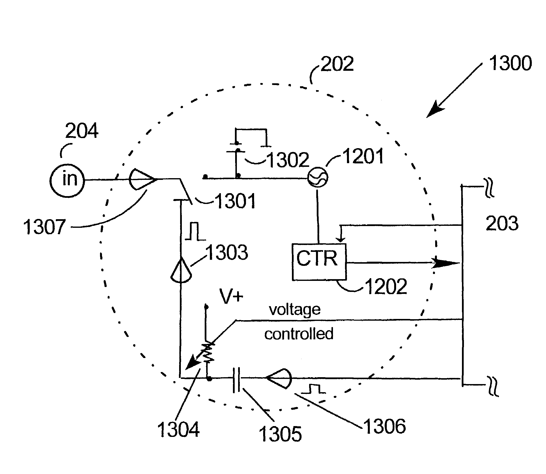
[0025]An example of a variable sized aperture window sampling system is also described. This example is achieved through the utilization of a variable aperture clock, such as a resistor capacitor differentiator comprised of a voltage controlled resistor and a capacitor. This variable aperture clock can modify the pulse width of a sample pulse to form a narrower pulse width, and therefore a faster sampling rate. This variable sized aperture window sampling system can be used by itself for ADC sampling, or it can be combined with any of the previously described multiple ADC distributed sampling systems.

Problems solved by technology

However, this reproduction is only possible if the sampling rate is higher than twice the highest frequency of the signal.
Building a chip with such a high sampling frequency is more costly, and the architecture of such chips does not permit embedding of large data functions such as CPUs, memory, etc. in such a chip.
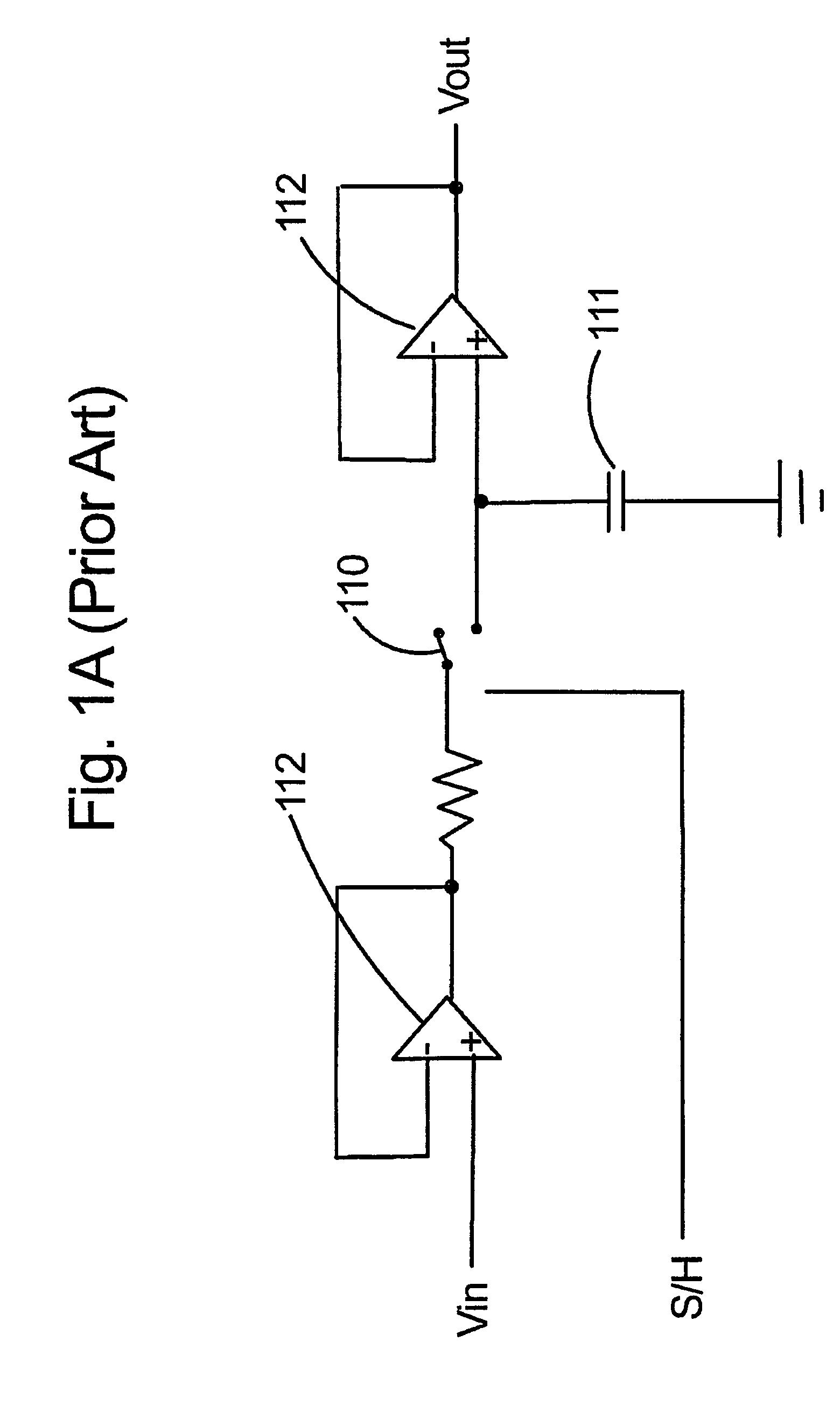
A sample and hold ADC is simple and reliable, but is limited in its sampling frequency rate and it has a high error probability.
This has the advantage of being a fast acting device, but has the disadvantage of being a large power consumption device.
The successive approximation ADC is a faster device, but has the disadvantages of high power consumption and a large number of components.

Method used


Image

  • Variable sized aperture window of an analog-to-digital converter
  • Variable sized aperture window of an analog-to-digital converter
  • Variable sized aperture window of an analog-to-digital converter

Examples


first embodiment

[0049]The time period between each ADC sampling of the input signal could be achieved in various ways, as exemplified by the following embodiments. FIG. 3a discloses a time relationship between samplings taken of an input signal 301 and taps in a trace pattern 303 of a time distributed sampling system in the invention. The trace pattern 303 contains a plurality of elongated wires connected in series. This time distributed sampling system has a plurality of ADC systems, wherein each ADC system comprises an ADC 202 and an associated central processing unit (CPU) 203, as discussed previously in relation to FIG. 2. When a timing signal 306 travels through a first length of wire 303a to a tap point of W1, a prompt to sample the input signal 301 after a measurable amount of time, given by Δt 304 is made. This timing is represented as ADC sampling point C1. As the timing signal 306 continues through a second length of wire 303b to a second tap point of W2, a prompt to sample the input sign...

second embodiment

[0052]FIG. 3b discloses a time relationship between samplings taken of an input signal 301 and taps made in a connected series of inverter pairs 305 of a time distributed sampling system in the invention. Each clocked trace pattern 303 of FIG. 3a is replaced with a pair of inverters 305 in FIG. 3b. A timing signal 306 travels through a series of connected inverter pairs 305. When the timing signal 306 travels through a first inverter pair 305a, a prompt to sample the input signal 301 after a first time period, Δt 304 is made, which coincides with the ADC sampling point C1. As the timing signal 306 continues through a second inverter pair 305b, a prompt to sample the input signal 301 after a second time period, Δt 304 is made, which coincides with the ADC sampling point, C2. A separate ADC system samples the input signal 301 at each of the ADC sampling points, C1 through Cn which occurs when the timing signal 306 travels through each inverter pair at points designated by W1 through W...

third embodiment

[0054]FIG. 4 discloses a time relationship between samplings taken of an input analog signal 405 and line taps made in a specific permittivity material device 401 in the invention. The time distribution sampling is achieved through the use of a specific permittivity material device 401, such as a surface acoustic wave (SAW) device. An input signal 405 is sampled after each measurable time period, Δt 403 as a timing signal 406 travels past each equi-distant point, given by S1 through Sn along the device 401.

[0055]The specific permittivity material device distributed sampling system represented by FIG. 4 works similar to the trace distributed sampling system of FIG. 3a. A separate ADC system contains an ADC and a corresponding CPU, as previously described with reference to FIG. 2. Each sequential ADC system samples the input signal 405, represented by ADC sampling points 402 when a timing signal 406 reaches each sequential equi-distant point along the device 401, corresponding to poin...


PUM


Abstract

An improvement in sampling a high frequency input analog signal and converting it to a digital output signal is disclosed. This is accomplished by using a multitude of analog-to-digital converters in conjunction with a distributed sampling system. This combination of multiple converters and a distributed sampling system allows use of conventional device processing, such as that of 0.18 micron silicon, and also provides accurate sampling of very high frequency input signals. The distributed sampling system provides multiple samplings of the input signal by using multiple ADCs for multiple samplings, wherein each sampling is sequentially offset a fixed amount of time from the most recent preceding sampling. Each ADC has a designated central processing unit (CPU) to obtain sufficient data transfer capabilities. The samplings from the multitude of ADCs are a series of sequential digital output values. The digital output values could be the result of samplings all at the same frequency, or at different frequencies. Types of distributed sampling systems include a multitude of elongated trace patterns interconnected in series, a multitude of inverter pairs interconnected in series, a specific permittivity material device, and a sequencer or multiplier. A second enhanced sampling system includes a variable sized aperture window, wherein a width of a sample pulse is narrowed through a variable clock mechanism to produce a faster sampling rate. This variable sized aperture window system can be used by itself, or in combination with any of the presently described multiple ADC distributed sampling systems.

Description

[0001]This application is a continuation-in-part of copending U.S. application Ser. No. 11 / 726,739 entitled “Analog-to-Digital Converter System with Increased Sampling Frequency,” which was filed Mar. 22, 2007 by the same inventors and is incorporated herein by reference in its entirety.BACKGROUND OF THE INVENTION[0002]1. Field of the Invention[0003]The present invention relates to the field of computers and computer processors, and more particularly to analog-to-digital converters (ADCs).[0004]2. Description of the Background Art[0005]An analog-to-digital converter (ADC) is an electronic circuit that converts continuous signals to discrete digital numbers. Typically, an ADC is an electronic device that converts an input analog voltage to a digital number.[0006]The analog signal is continuous in time and it is necessary to convert this to a flow of digital values. It is therefore required to define the rate at which new digital values are sampled from the analog signal. The rate of ...

Claims


Application Information

Patent Timeline
Patent Type & Authority Patents(United States)
IPC IPC(8): H03M1/00
CPCH03M1/1245H03M1/1215H03M1/60H03M1/12
Inventor MOORE, CHARLES H.SNIVELY, LESLIE O.HUIE, JOHN
Owner ARRAY PORTFOLIO
Why Eureka
Try Eureka