Mismatch-shaping dynamic element matching systems and methods for multi-bit sigma-delta data converters

a dynamic element matching and dynamic element technology, applied in transmission systems, instruments, code conversion, etc., can solve the problems of limiting the achievable maximum input signal bandwidth, and reducing the maximum allowable input range, so as to achieve the effect of reducing the delay introduced by the dem algorithm, reducing the delay, and facilitating higher-order spectral shaping of mismatch errors

Active Publication Date: 2009-08-18
INTRINSIX
View PDF53 Cites 16 Cited by
  • Summary
  • Abstract
  • Description
  • Claims
  • Application Information

AI Technical Summary

Benefits of technology

[0016]In one aspect, at least some embodiments of the invention relate to multi-bit sigma-delta data converters employing dynamic element matching (DEM) in a particular way, and the corresponding methods, which can help to reduce the effects of the component mismatch errors due to the internal multi-bit quantizer.
[0035]In high-speed continuous-time implementations of at least some SDM ADC systems implemented in accordance with the invention, the additional delay incurred in the feedback loop, by the conventional feedback DEM methods (as cited above), usually limits the maximum achievable sampling frequency and the input signal bandwidth. In at least some embodiments of the invention described herein, however, the DEM circuit is included in the feed-forward path of the SDM, helping to eliminate the need for additional DEM circuits in the sensitive feedback path. Consequently, no additional delay is incurred in the feedback path of the SDM. This advantage of this embodiment of present invention makes it particularly suitable in high-speed continuous-time implementations of the SDM ADCs.

Problems solved by technology

One drawback of at least some single-bit SDMs, however, is that to obtain a higher resolution or wider bandwidth, a higher-order feedback loop is used, which in turn can cause stability problems and significantly reduce the maximum allowable input range.
Also, the required oversampling ratio (OSR, where OSR is defined as the ratio between the sampling rate of the output to the two times the input signal bandwidth) can be high, limiting the achievable maximum input signal bandwidth (because of the maximum attainable sampling frequency in a given VLSI technology).
Therefore, component mismatches in the multi-bit feedback DAC can severely limit the achievable resolution.
Achieving 16-bit linearity from a multi-bit DAC in digital Complementary Metal-Oxide Semiconductor (CMOS) technologies can be difficult unless expensive laser trimming or calibration techniques are used.
In some cases, known conventional methods have been limited to second-order mismatch-shaping due to difficulty and complexity in the design of higher-order mismatch-shaping algorithms.
In addition, the second-order mismatch-shaping can suffer from digital hardware overhead.
The hardware complexity of the second-order mismatch-shaping DEMs scales exponentially with the number of unit elements in the feedback DAC.
The extension of the second-order mismatch-shaping DEM to third and higher-order cases has problems due to the stability issues in the mismatch-shaping algorithm, and requires complex hardware, as described in the prior art.

Method used


Image

  • Mismatch-shaping dynamic element matching systems and methods for multi-bit sigma-delta data converters
  • Mismatch-shaping dynamic element matching systems and methods for multi-bit sigma-delta data converters
  • Mismatch-shaping dynamic element matching systems and methods for multi-bit sigma-delta data converters

Examples


Embodiment Construction

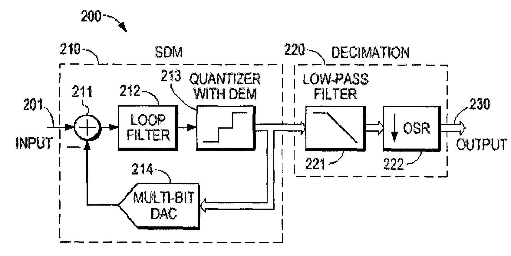
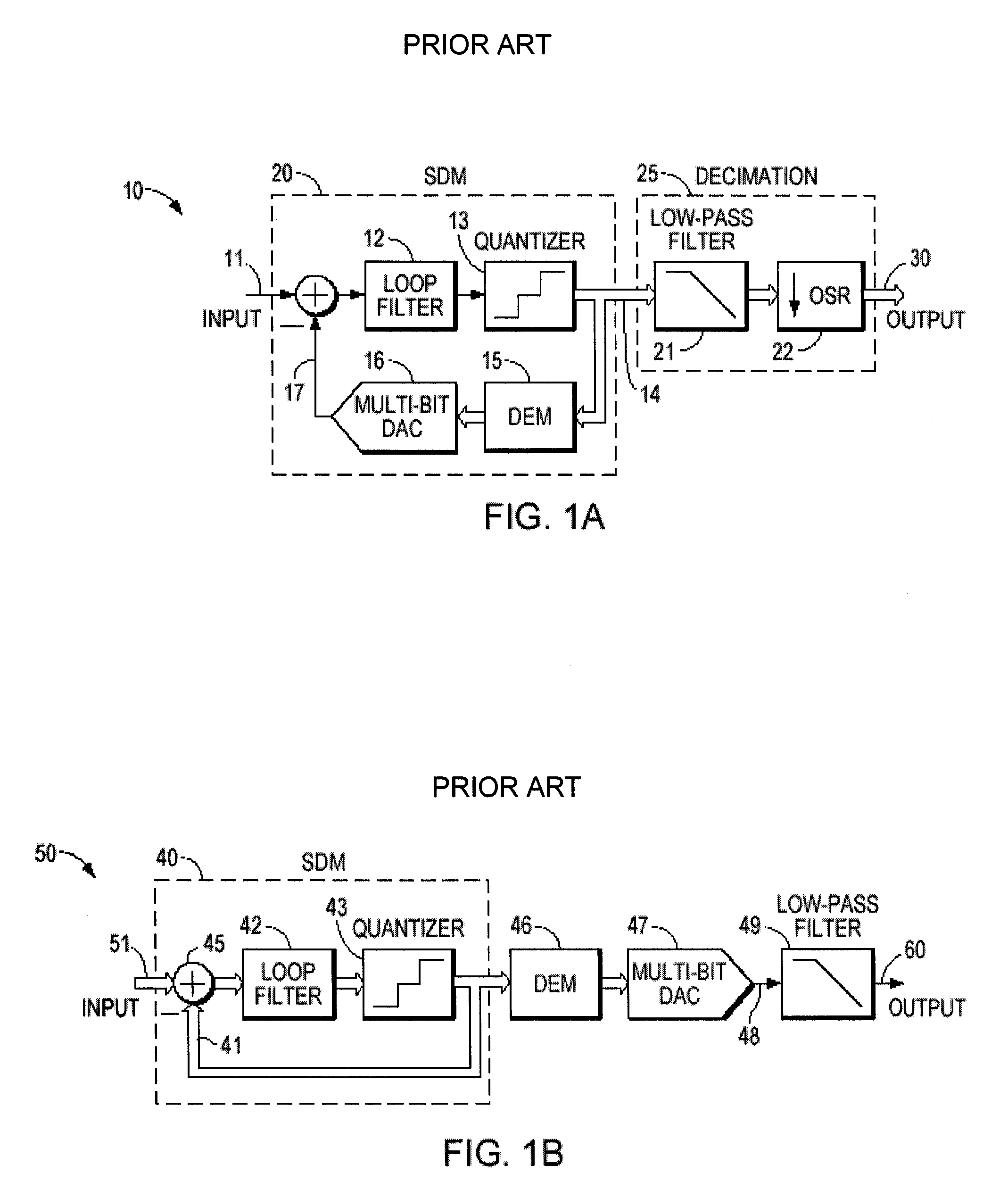
[0053]FIG. 1A is an illustrative block diagram of a prior art SDM ADC system, showing a top-level architecture for an SDM ADC system 10. An analog input signal 11 in an SDM 20 is subtracted from an analog feedback signal 17, and then processed by an analog feed-forward loop filter 12 before being fed into a multi-bit quantizer 13. The loop filter 12 (which can, for example, be an integrator) filters the resultant signal so as to minimize the effect of the error signal on a noise-shaping characteristic of the SDM 200. The multi-bit quantizer produces a low-resolution high-speed digital signal 14, which is converted in the feedback loop into the analog domain by a multi-bit feedback DAC 16. A digital decimation filter 25 processes the low-resolution and high-speed digital output from the multi-bit quantizer to produce a high-resolution low speed digital signal 30 at the output of the SDM ADC system.

[0054]Still referring to FIG. 1A, the analog input signal 11 to the SDM ADC system 10 h...


PUM


Abstract

A sigma delta modulator (SDM) data converter system is provided. The SDM data converter system comprises a signal path, a feedback signal path, and a multi-bit quantizer disposed in a feedforward path. The signal path receives an input signal to be processed. The feedback signal path provides a feedback signal that is subtracted from the input signal. The multi-bit quantizer is disposed in the feedforward path so as to receive the input signal after the feedback signal has been subtracted from it. Te multi-bit quantizer uses feedforward dynamic element matching (DEM) to spectrally shape mismatch errors in the SDM data conversion system and produce an output signal, wherein the output signal of the multi-bit quantizer is used for at least a portion of the feedback signal.

Description

Cross-Reference to Related Applications[0001]This patent application claims priority to a provisional patent application serial number 60 / 792,573, filed Apr. 16, 2006, entitled “Mismatch-Shaping Dynamic Element Matching Method For Multi-Bit Sigma-Delta Data Converters,” by Mucahit Kozak, Eugene M. Petilli, and Brian Jadus. The contents of this provisional patent application are hereby incorporated by reference.[0002]This patent application is a continuation-in-part of non-provisional patent application Ser. No. 11 / 208,430, filed Aug. 19, 2005, entitled “Hybrid Heterodyne Transmitters and Receivers,” by Eugene M. Petilli, Brian Jadus, Clyde Washburn, and John M. Alvermann. The contents of this nonprovisional patent application are hereby incorporated by reference.STATEMENT REGARDING FEDERALLY SPONSORED RESEARCH[0003]Not applicableFIELD OF THE INVENTION[0004]The present invention relates generally to sigma delta converters, and, in particular, to multi-bit sigma-delta data converters ...

Claims


Application Information

Patent Timeline
Patent Type & Authority Patents(United States)
IPC IPC(8): H03M3/00
CPCH03M1/0663H03M1/361H03M3/458H03M3/50H03M3/424H03M7/3026
Inventor PETILLI, EUGENE M.KOZAK, MUCAHITJADUS, BRIAN
Owner INTRINSIX
Why Eureka
Try Eureka