Monolithic semiconductor ceramic capacitor having varistor function and method for manufacturing monolithic semiconductor ceramic capacitor

a semiconductor ceramic capacitor and monolithic technology, applied in the direction of fixed capacitors, basic electric elements, electrical appliances, etc., can solve the problems of compact capacitors with low capacitance breaking, etc., and achieve good dielectric strength, good insulating properties, and good electric properties

Inactive Publication Date: 2009-09-01
MURATA MFG CO LTD
View PDF9 Cites 18 Cited by
  • Summary
  • Abstract
  • Description
  • Claims
  • Application Information

AI Technical Summary

Benefits of technology

[0036]A monolithic semiconductor ceramic capacitor having a varistor function according to the present invention includes semiconductor ceramic layers made of a semiconductor ceramic that has a Sr site, a Ti site, crystal grains, and grain boundary layers. The semiconductor ceramic satisfies the inequality 1.000<m≦1.020, wherein m represents the molar ratio of the Sr site to the Ti site. The crystal grains contain a donor element such as La, Sm, Dy, Ho, Y, Nd, Ce, Nb, Ta or W in the form of a solid solution. The grain boundary layers contain an acceptor element such as Mn, Co, Ni or Cr. The amount of the acceptor element therein is greater than 0 mol and equal to or less than 0.5 mol (preferably 0.3 to 0.5 mol) per 100 mol of Ti. The crystal grains have an average size of 1.0 μm or less (preferably 0.5 to 0.8 μm). Therefore, the monolithic semiconductor ceramic capacitor has a large apparent dielectric constant ∈rAPP, good electric properties, good insulating properties, and good dielectric strength and is suitable for thin or compact apparatuses. Although the monolithic semiconductor ceramic capacitor is compact and has low capacitance, the monolithic semiconductor ceramic capacitor has good dielectric strength.
[0037]A method for manufacturing monolithic semiconductor ceramic capacitor according to the present invention includes a pre-fired powder-preparing step of weighing ceramic raw materials including a donor compound such that the inequality 1.000<m≦1.020 holds, mixing the ceramic raw materials, and then pre-firing the mixture to prepare a pre-fired powder, where m represents the molar ratio of a Sr site to a Ti site; a heat-treated powder-preparing step of weighing an acceptor element such that the amount of the acceptor element is greater than 0 mol and equal to or less than 0.5 mol per 100 mol of Ti, mixing the acceptor element with the pre-fired powder, and then heat-treating this mixture to prepare a heat-treated powder; a laminate-preparing step of forming green ceramic sheets from the heat-treated powder and then alternately stacking the green ceramic sheets and internal electrode layers to prepare a laminate; and a firing step of primarily firing the laminate in a reducing atmosphere and then secondarily firing the resulting laminate in a slight reducing, air, or oxidizing atmosphere. Therefore, the monolithic semiconductor ceramic capacitor can be efficiently manufactured.

Problems solved by technology

Therefore, the application of the high-voltage pulses or static electricity to the electronic devices can cause the malfunction of the electronic devices or the breakage of semiconductor elements and can particularly cause the breakage of compact capacitors having low capacitance.

Method used


Image

  • Monolithic semiconductor ceramic capacitor having varistor function and method for manufacturing monolithic semiconductor ceramic capacitor
  • Monolithic semiconductor ceramic capacitor having varistor function and method for manufacturing monolithic semiconductor ceramic capacitor

Examples


example 1

[0093]The following ceramic raw materials were prepared: SrCO3, LaCl3 and particles of TiO2. The TiO2 particles had a specific surface area of 30 m2 / g (an average size of about 30 nm). LaCl3 was weighed such that the content of La was 1.2 mol per 100 mol of Ti. SrCO3 and TiO2 were weighed such that the molar ratio of the Sr site to the Ti site was as shown in Table 1. Three parts by weight of an ammonium polycarboxylate serving as a dispersant was added to 100 parts by weight of the weighed compounds. The mixture was charged into a ball mill together with PSZ balls, serving as boulders, having a diameter of 2 mm and pure water and then wet-mixed for 16 hours in the ball mill, whereby slurry was prepared.

[0094]The slurry was dried and then pre-fired at 1350° C. for two hours in an air atmosphere, whereby a pre-fired powder with crystal grains containing La in the form of a solid solution was obtained.

[0095]MnCO3, tetraethoxysilane (Si(OC2H5)4) and a dispersant were added to the pre-f...

example 2

[0119]Samples 41 to 49 different in size and / or capacitance were prepared using a semiconductor ceramic having the same composition as that of the semiconductor ceramic used to prepare Sample 22 described in Example 1 and were then evaluated.

[0120]A ceramic slurry having the same composition as that of the slurry used to prepare Sample 22 by the same procedure as that described in Example 1 was employed.

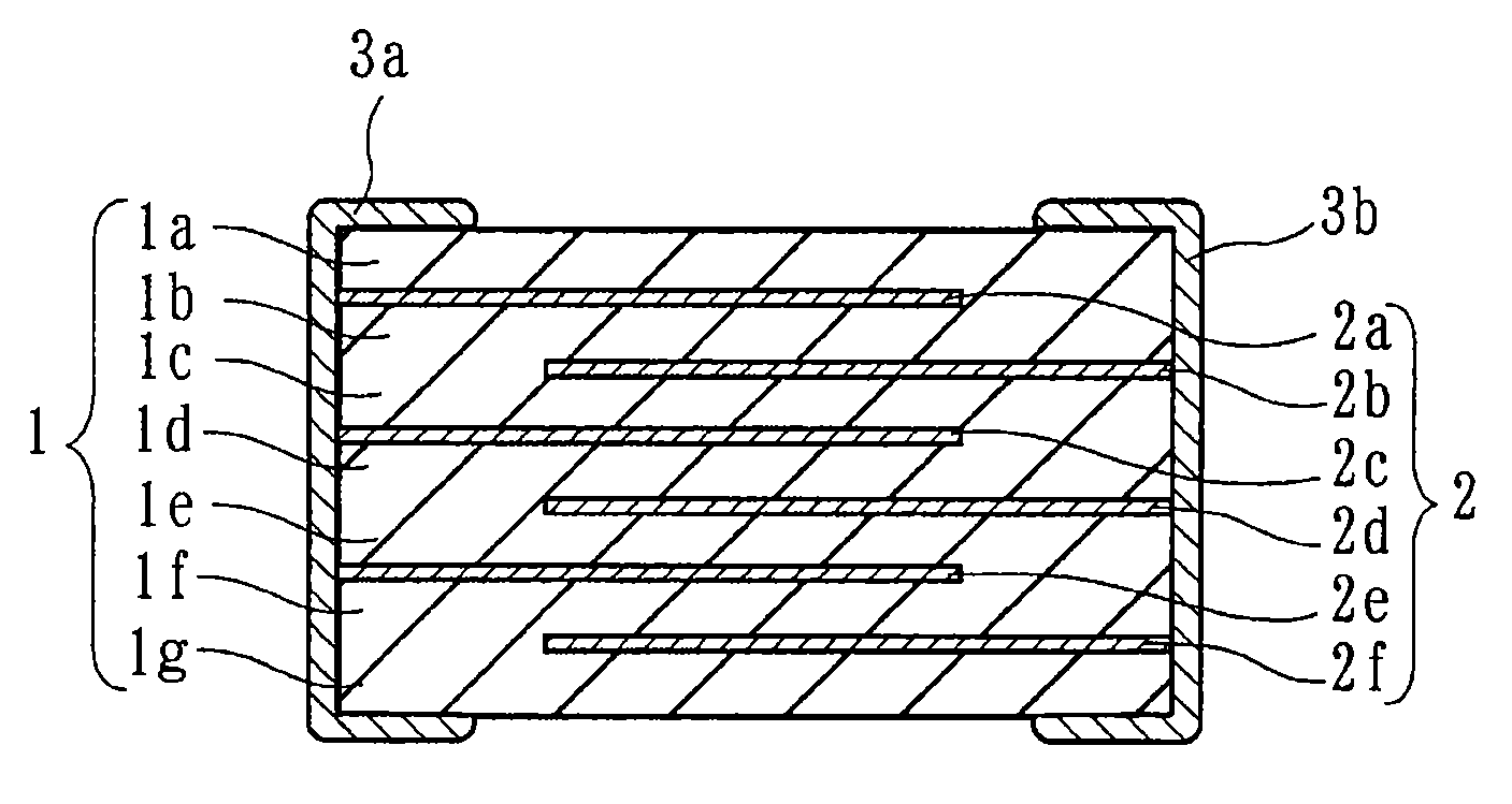
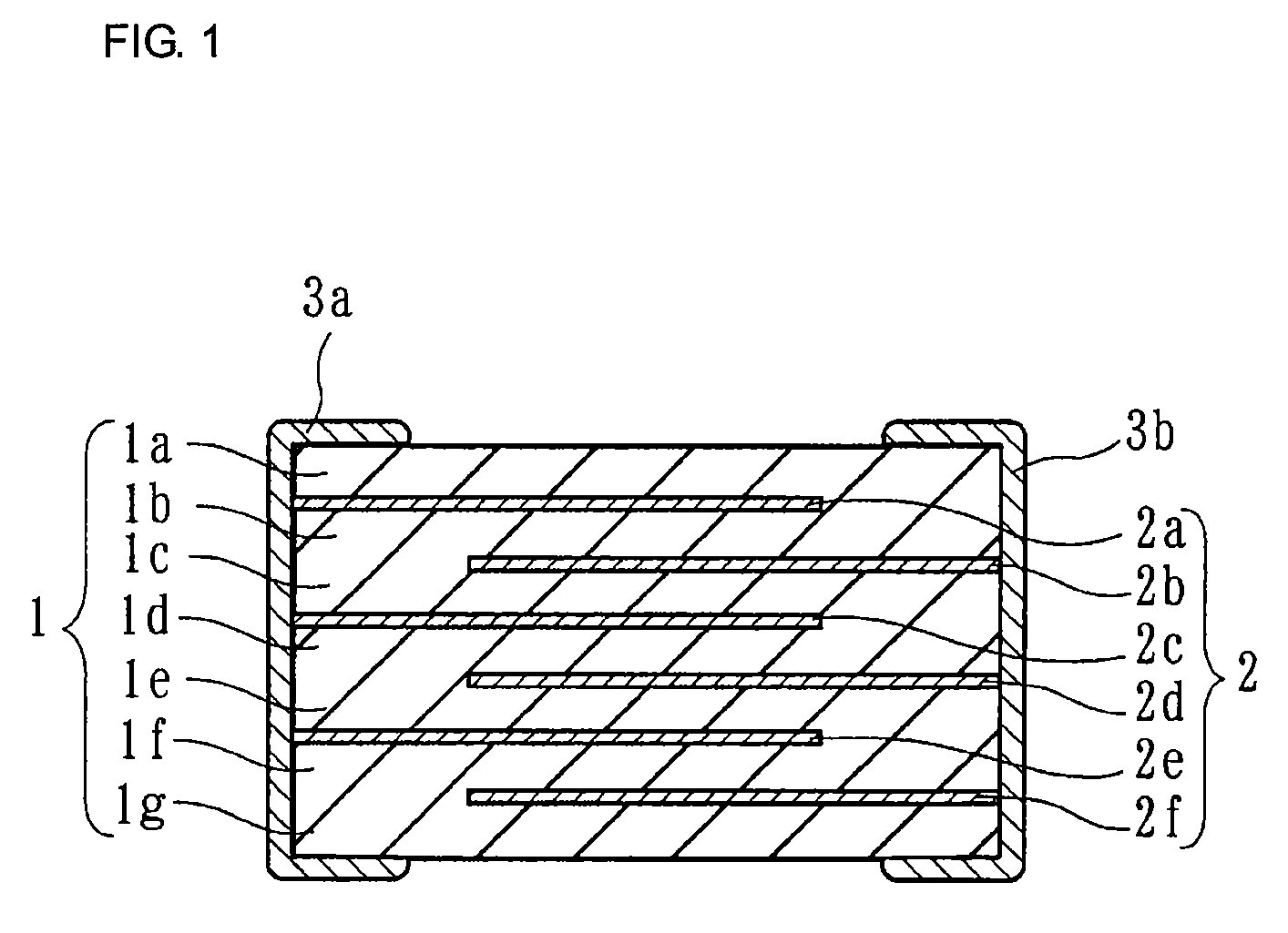
[0121]The ceramic slurry was formed into green ceramic sheets by a lip coating process. An internal electrode-forming conductive paste principally containing Ni was applied onto some of the green ceramic sheets by screen printing, whereby a conductive layer having a predetermined pattern was formed on each green ceramic sheet.

[0122]A number of the green ceramic sheets having the conductive layers were stacked in a predetermined direction. The stacked green ceramic sheets were sandwiched between the green ceramic sheets having no conductive layer. These ceramic green sheets were press...


PUM

PropertyMeasurementUnit
sizeaaaaaaaaaa
sizeaaaaaaaaaa
molar ratioaaaaaaaaaa

Abstract

A monolithic semiconductor ceramic capacitor includes semiconductor ceramic layers made of a semiconductor ceramic having a Sr site and a Ti site. The semiconductor ceramic satisfies the inequality 1.000<m≦1.020, wherein m represents the molar ratio of the Sr site to the Ti site. The semiconductor ceramic contains crystal grains and has grain boundary layers. The crystal grains contain a donor element such as La or Sm in the form of a solid solution. The grain boundary layers contain an acceptor element such as Mn, Co, Ni or Cr. The amount of the acceptor element therein is equal to or less than 0.5 mol (preferably 0.3 to 0.5 mol) per 100 mol of Ti. The crystal grains have an average size of 1.0 μm or less (preferably 0.5 to 0.8 μm). Therefore, the monolithic semiconductor ceramic capacitor has good electrical properties, good resistivity, good dielectric strength, and high reliability and is suitable for thin or compact apparatuses.

Description

[0001]This is a continuation of application Serial No. PCT / JP2007 / 061106, filed May 31, 2007.TECHNICAL FIELD[0002]The present invention relates to monolithic semiconductor ceramic capacitors having a varistor function and methods for manufacturing the monolithic semiconductor ceramic capacitors. The present invention particularly relates to a monolithic semiconductor ceramic capacitor which has a varistor function, which is of a boundary insulative layer type, and which contains SrTiO3 and also relates to a method for manufacturing the monolithic semiconductor ceramic capacitor.BACKGROUND ART[0003]Developments in electronics has led to the widespread use of mobile electronic devices such as mobile phones and notebook personal computers and vehicle-mounted electronic devices. Compact multi-functional electronic devices have been recently demanded.[0004]In order to manufacture the compact multi-functional electronic devices, various semiconductor elements such as ICs and LSIs are used...

Claims


Application Information

Patent Timeline
Patent Type & Authority Patents(United States)
IPC IPC(8): H01G4/06
CPCB32B18/00C04B35/47H01C7/115H01C7/18H01G4/1227H01G4/1281H01G4/30B82Y30/00Y10T29/435C04B2235/3224C04B2235/3225C04B2235/3227C04B2235/3229C04B2235/3241C04B2235/3251C04B2235/3258C04B2235/326C04B2235/3262C04B2235/3275C04B2235/3279C04B2235/3281C04B2235/3418C04B2235/36C04B2235/441C04B2235/5409C04B2235/5454C04B2235/6025C04B2235/6582C04B2235/663C04B2235/785C04B2235/786C04B2235/79C04B2235/85H01G4/12C04B35/46H01C7/10
Inventor TANI, SHINSUKEKAWAMOTO, MITSUTOSHI
Owner MURATA MFG CO LTD
Why Eureka
Try Eureka