Semiconductor device and manufacturing method thereof

a technology of semiconductor devices and manufacturing methods, applied in the direction of semiconductor devices, basic electric elements, electrical appliances, etc., can solve the problems of difficult formation of ldd regions having a width of 0.5 m or more in self-alignment manner, and achieve the effect of increasing the number of manufacturing steps, reducing parasitic capacitance or parasitic resistance, and high operational performan

Inactive Publication Date: 2009-09-15
SEMICON ENERGY LAB CO LTD
View PDF50 Cites 36 Cited by
  • Summary
  • Abstract
  • Description
  • Claims
  • Application Information

AI Technical Summary

Benefits of technology

[0017]The present invention provides a TFT including at least one LDD region in a self-alignment manner without forming a sidewall spacer and increasing the number of manufacturing steps.
[0041]In addition, a width of an LDD region formed only on one side of a channel formation region can be 0.5 μm or more, preferably 1.5 to 2 μm, further 2 μm or more. Therefore, in accordance with the present invention, a semiconductor device provided with a circuit having high operational performance and reliability can be achieved.

Problems solved by technology

Therefore, according to the techniques disclosed in Patent Documents 1, 2, and 3, it is also difficult to form an LDD region having a width of 0.5 μm or more in a self-alignment manner.

Method used


Image

  • Semiconductor device and manufacturing method thereof
  • Semiconductor device and manufacturing method thereof
  • Semiconductor device and manufacturing method thereof

Examples


embodiment mode 1

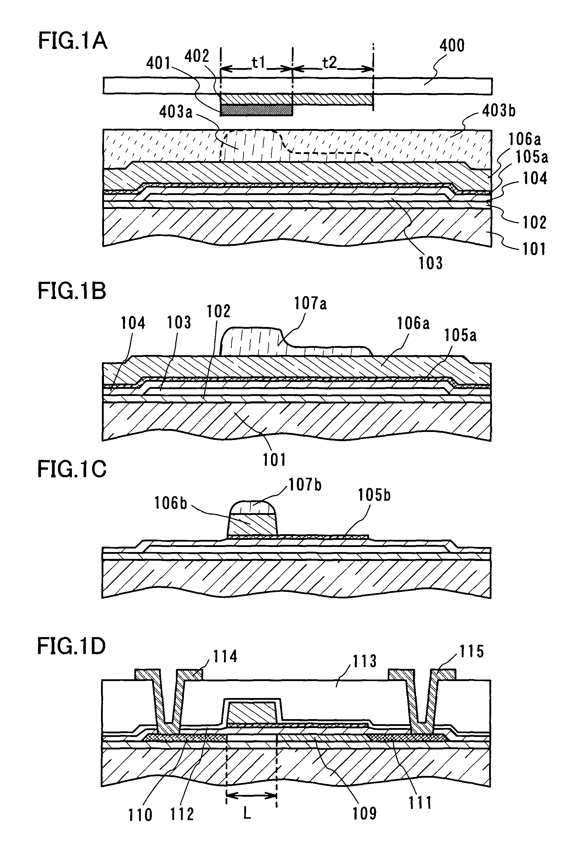
[0055]This embodiment mode shows a step of forming a low-concentration impurity region in a self-alignment manner only on one side of a channel formation region by using a gate electrode of a TFT as a mask in ion-doping.

[0056]First, a first insulating film (a base insulating film) 102 is formed over a substrate 101 having an insulating surface. The substrate 101 having an insulating surface can be a light-transmitting substrate, for example, a glass substrate, a crystallized glass substrate, or a plastic substrate. When a thin film transistor that will be formed later is applied to a top emission light-emitting display device or a reflective liquid crystal display device, a ceramic substrate, a semiconductor substrate, a metal substrate, or the like can also be used.

[0057]The first insulating film 102 can be formed by using an insulating film such as a silicon oxide film, a silicon nitride film, or a silicon oxynitride (SiOxNy) film. Subsequently, a semiconductor layer 103 is formed...

embodiment mode 2

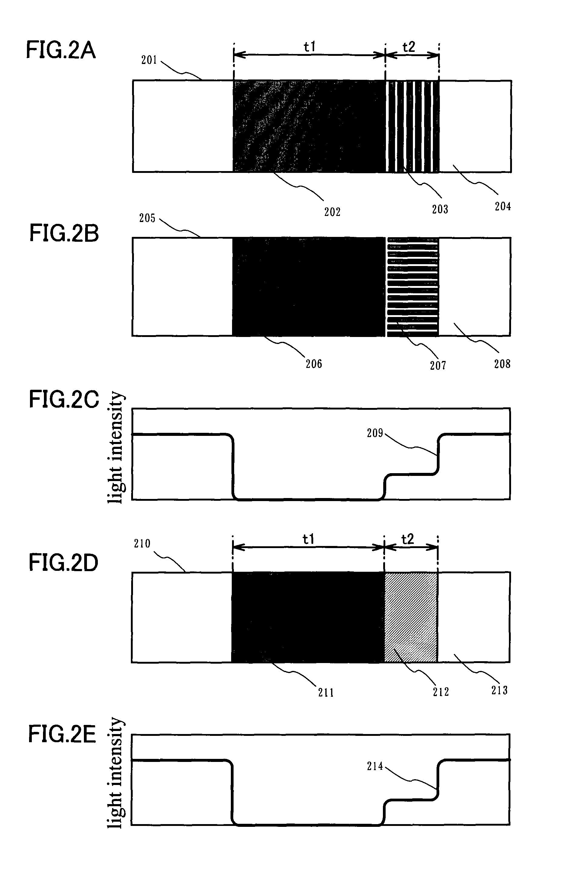
[0105]In this embodiment mode, an exposure mask provided with an assist pattern that is formed of a diffraction grating pattern or a semi-transmitting film and has a function of reducing light intensity, which is used in Embodiment Mode 1, will be explained with reference to FIGS. 2A to 2E.

[0106]It is to be noted that FIG. 1A shows a cross-sectional view of an exposure mask. Similarly, also in FIGS. 2A to 2E, a width of a light-shielding portion is referred to as t1, and a width of a portion provided with an assist pattern is referred to as t2.

[0107]As specific examples of the assist pattern, FIGS. 2A and 2B show part of top views of an exposure mask provided with a diffraction grating pattern having a slit portion formed of a line and a space, which are equal to or lower than a resolution limit of an exposure apparatus. A slit direction of the slit portion may be parallel to a direction of a main pattern (a light-shielding portion 202) like a slit portion 203, or may be perpendicul...

embodiment mode 3

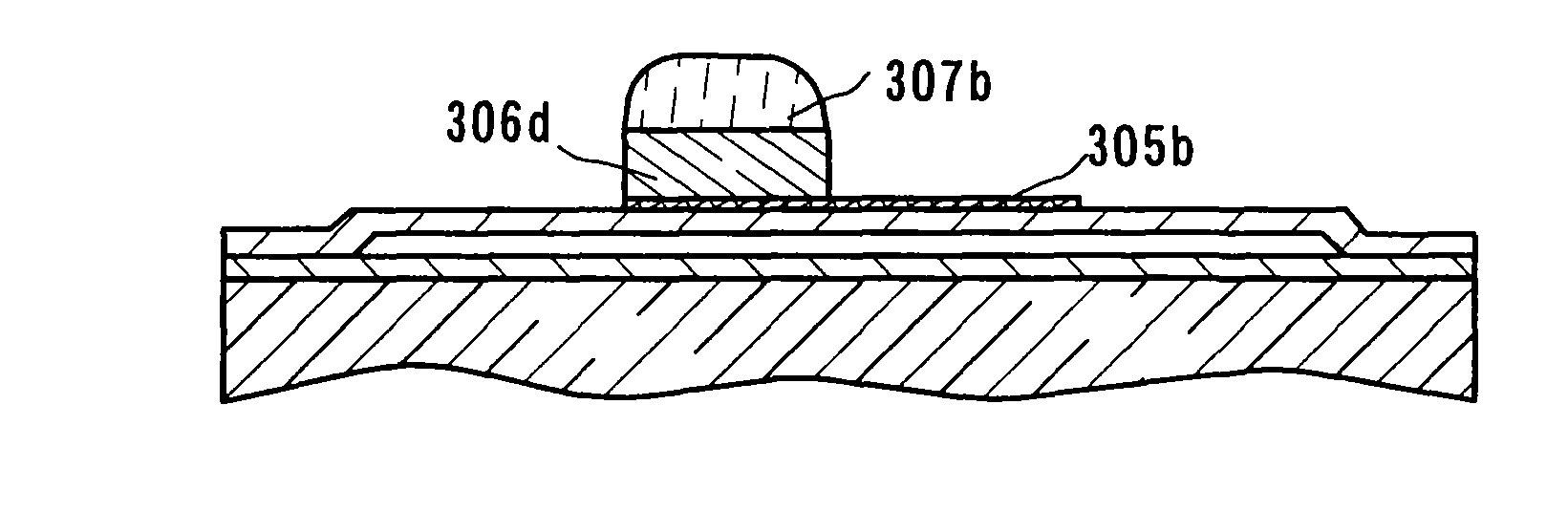
[0113]A method for forming a conductive stacked pattern shown in Embodiment Mode 1 is not particularly limited. Here, an example of forming a conductive stacked pattern by changing etching conditions several times during the steps will be explained with reference to FIGS. 3A to 3F.

[0114]First, similarly to Embodiment Mode 1, a resist pattern 307a is formed over a second conductive layer 306a. FIG. 3A corresponds to FIG. 1B.

[0115]In FIG. 3A, over a substrate 301, a first insulating film (a base insulating film) 302, a semiconductor layer 303, a second insulating film (a gate insulating film) 304, a first conductive layer 305a, and the second conductive layer 306a are formed.

[0116]Then, as shown in FIG. 3B, etching is performed with a first etching condition using the resist pattern 307a as a mask to remove part of the second conductive layer, and thus, a second conductive layer 306b is formed. It is to be noted that the second conductive layer 306b is formed over the entire surface a...


PUM


Abstract

The present invention provides a TFT including at least one LDD region in a self-alignment manner without forming a sidewall spacer and increasing the number of manufacturing steps. A photomask or a reticle provided with an assist pattern that is formed of a diffraction grating pattern or a semi-transmitting film and has a function of reducing light intensity is employed in a photolithography step of forming a gate electrode, an asymmetrical resist pattern having a region with a thick thickness and a region with a thickness thinner than that of the above region on one side is formed, a gate electrode having a stepped portion is formed, and an LDD region is formed in a self-alignment manner by injecting an impurity element to the semiconductor layer through the region with a thin thickness of the gate electrode.

Description

BACKGROUND OF THE INVENTION[0001]1. Field of the Invention[0002]The present invention relates to a semiconductor device including a circuit formed by using a thin film transistor (hereinafter also referred to as a TFT) and a manufacturing method thereof. For example, the present invention relates to an electronic device provided with, as a component, an electrooptic device typified by a liquid crystal display panel or a light-emitting display device having an organic light-emitting element.[0003]In this specification, a semiconductor device generally refers to a device which can function by utilizing semiconductor characteristics, and an electrooptic device, a semiconductor circuit, and an electronic device are all semiconductor devices.[0004]2. Description of the Related Art[0005]In recent years, a technique for forming a thin film transistor (TFT) using a semiconductor thin film (several nm to several hundred nm) formed over a substrate having an insulating surface has attracted a...

Claims


Application Information

Patent Timeline
Patent Type & Authority Patents(United States)
IPC IPC(8): H01L21/00H01L21/84
CPCH01L27/1214H01L27/1288H01L29/78624H01L29/66757H01L27/124H01L27/12H01L29/42384
Inventor OHNUMA, HIDETOMONOE, SHIGEHARUYAMAZAKI, SHUNPEI
Owner SEMICON ENERGY LAB CO LTD
Why Eureka
Try Eureka