Two-dimensional photonic crystal optical multiplexer/demultiplexer

a two-dimensional, photonic crystal technology, applied in the direction of optical waveguide light guide, instruments, nanotechnology, etc., can solve the problems the photonic band gap, and the inability to propagate light, so as to increase the degree of freedom, decrease the q-factor, and the effect of reducing the q-factor

Inactive Publication Date: 2009-09-15
JAPAN SCI & TECH CORP
View PDF11 Cites 3 Cited by
  • Summary
  • Abstract
  • Description
  • Claims
  • Application Information

AI Technical Summary

Benefits of technology

[0026]The low refractive index area may be created by embedding a material having a low refractive index in the body or just forming a hole in the body. In the latter case, the air constitutes the modified refractive index area. Practically, air is the material that has the lowest refractive index. Therefore, forming a hole is advantageous to increase the difference in the refractive index between the modified refractive index area and the body. Furthermore, forming a hole is easier than embedding a different material.
[0043]The principal object of the second mode of the present invention is to increase the degree of freedom for the donor type defects, which are created by not boring holes in the body. This construction of the second mode is also applicable to the acceptor type defect and provides a specific advantage for it. When two or more wavelengths of light are to be mixed or separated by acceptor type defects created by increasing the diameter of the hole at a certain lattice point, it has been conventionally necessary to form plural holes having different diameters in a single body slab. This construction, however, decreases the Q-factor. The second mode of the present invention can be preferably used to avoid such a decrease in Q-factor. That is, in plural forbidden band zones, modified refractive index areas are formed with different arrangement cycles corresponding to the plural wavelengths for optical multiplexing / demultiplexing. The ratio of the size of the modified refractive index area in one forbidden band zone to that in another, and the ratio of the size of the acceptor type point defect placed in one forbidden band zone to that in another, are set equal to the predetermined ratio of the arrangement cycle of the modified refractive index areas in the former forbidden band zone to that in the latter. This construction enables the multiplexing / demultiplexing of plural wavelengths of light without decreasing the Q-factor.
[0044]In the first mode of the present invention, the introduction of a cluster defect enables a multiplexer / demultiplexer to have higher Q-factor than in the case of using a point defect composed of a single lattice point. This is because the presence of the cluster defect increases the effective refractive index around the defect, which improves the light confining efficiency. The optical multiplexer / demultiplexer also exhibits high efficiency when it has asymmetry in the orthogonal direction or when it is used to produce polarized light.
[0045]In the second mode of the present invention, the in-plane heterostructure provides a higher degree of freedom for the selection of wavelengths for the multiplexing / demultiplexing of light even in the case of using donor type defects. The Q-factor obtained thereby is approximately equal to that of a photonic crystal for the multiplexing / demultiplexing of a single wavelength of light. When the donor type defect having a high Q-factor according to the first mode is used to construct the structure of the second mode, it will be relatively easy to obtain a device for multiplexing / demultiplexing various wavelengths of light with a high Q-factor. The second mode can also be effectively applied to the acceptor type defect.

Problems solved by technology

One of its particular features is that it has an energy region (called the photonic bandgap) that does not allow the propagation of light.
The decrease in Q-factor may also result from asymmetry that may be introduced into a point defect.

Method used


Image

  • Two-dimensional photonic crystal optical multiplexer/demultiplexer
  • Two-dimensional photonic crystal optical multiplexer/demultiplexer
  • Two-dimensional photonic crystal optical multiplexer/demultiplexer

Examples


Embodiment Construction

(1) Embodiment of the First Mode

(1-1) Construction

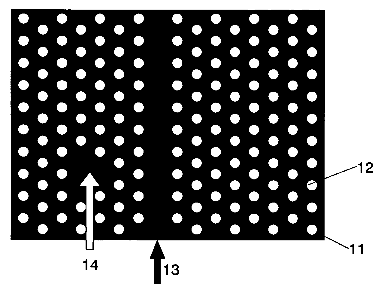
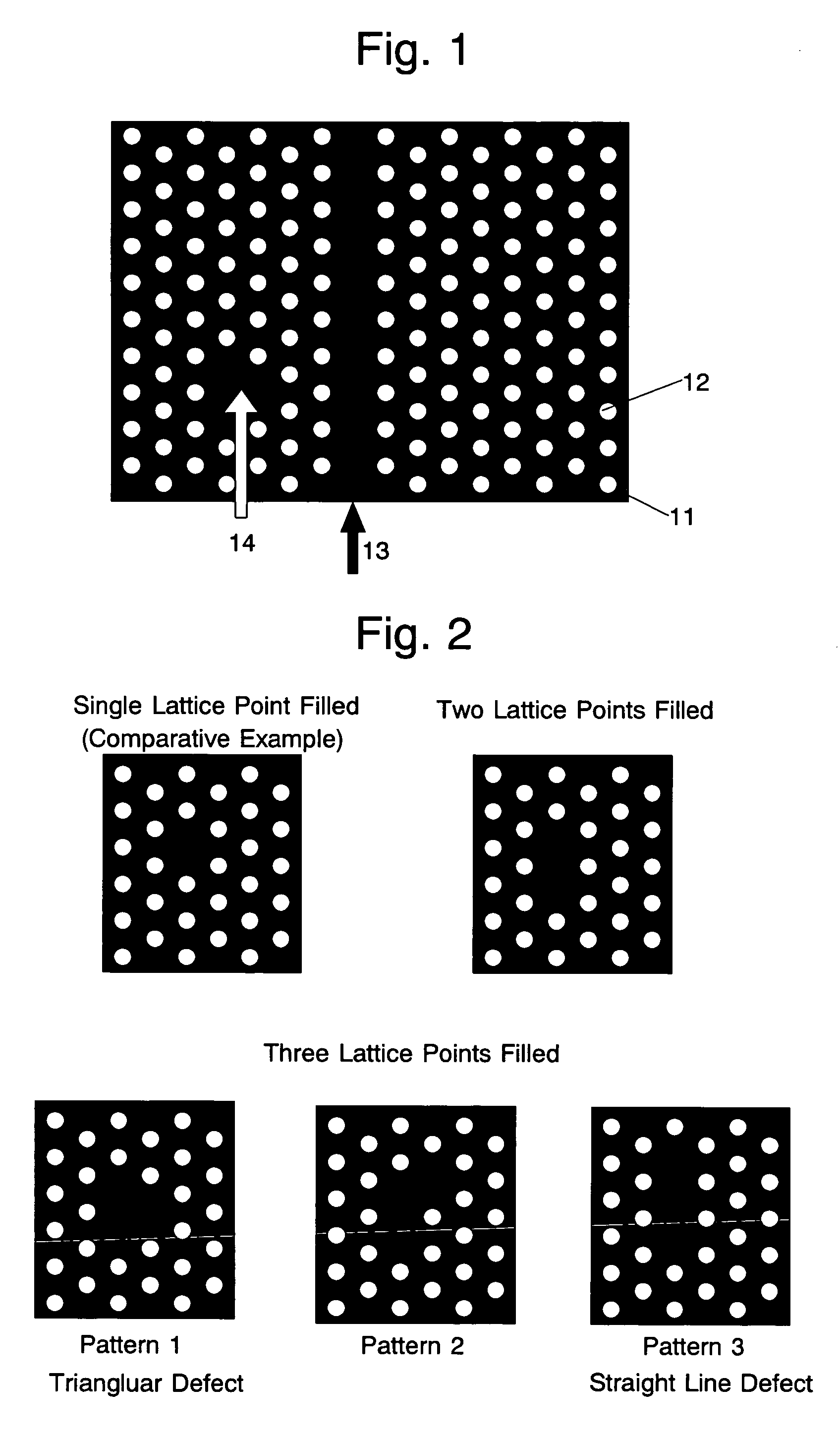
[0065]As an embodiment of the first mode of the present invention, a two-dimensional photonic crystal as schematically illustrated in FIG. 1 is described. The plate shown in FIG. 1 is a slab (or body) 11. For infrared light having a wavelength λ=1.55 μm used in normal optical communications, the slab 11 may be made from InGaAsP, which is transparent to that wavelength of infrared light. The slab 11 has holes 12 periodically arranged as the modified refractive index areas (or low refractive index areas) as shown by the white circles. The holes 12 shown in FIG. 1 are arranged in a triangular lattice pattern, which may be arranged in various patterns, such as a square lattice pattern.

[0066]Waveguide 13 is formed by not boring holes along a linear zone indicated by the solid arrow in FIG. 1. A donor type cluster defect 14 is formed by not boring holes at plural lattice points within the area indicated by the white arrow. In the following...


PUM

PropertyMeasurementUnit
wavelength resolutionaaaaaaaaaa

Abstract

The present invention provides an optical multiplexer / demultiplexer that can be smaller in size and higher in Q-factor or efficiency. This object is achieved by the following construction. In a slab-shaped body 11, low refractive index areas 12 having a refractive index lower than that of the material of the body 11 are periodically arranged to construct a two-dimensional photonic crystal, in which a waveguide 13 is formed by not boring holes 12 linearly. A donor type cluster defect 14 is formed by not boring holes 12 at two ore more lattice points located adjacent to the waveguide 13. With this construction, only a specific wavelength of light included in the light propagating through the waveguide 13 resonates at the donor type cluster 14, and the light thus trapped is released to the outside (demultiplexing). Conversely, only a specific wavelength of light may be introduced through the donor type cluster defect 14 into the waveguide 13 (multiplexing).

Description

TECHNICAL FIELD[0001]The present invention relates to an optical multiplexing / demultiplexing device used for wavelength division multiplexing communication.BACKGROUND ART[0002]Recently, photonic crystals have been drawing attentions as a new optical device. A photonic crystal is an optical functional material having a periodic distribution of refractive index, which provides a band structure with respect to the energy of photons. One of its particular features is that it has an energy region (called the photonic bandgap) that does not allow the propagation of light.[0003]An example of the application fields of the photonic crystal is the optical communication. Recent optical communications use the wavelength division multiplexing (WDM) in place of a conventional method called the time division multiplexing (TDM). The wavelength division multiplexing is a communication method in which plural wavelengths of light, each carrying a different signal, propagate through a single transmissi...

Claims


Application Information

Patent Timeline
Patent Type & Authority Patents(United States)
IPC IPC(8): G02B6/10G02B6/122G02B6/12G02B6/34G02F1/00
CPCG02B6/1225B82Y20/00
Inventor NODA, SUSUMUMOCHIZUKI, MASAMITUASANO, TAKASHI
Owner JAPAN SCI & TECH CORP
Why Eureka
Try Eureka