Adhesive injection apparatus

a technology of adhesive injection and injection apparatus, which is applied in the direction of application, manufacturing tools, drawing profiling tools, etc., can solve the problems of increasing wasting the peripheral edge portion of the stacked wafer located above and below the sealing section, and the inability to inject adhesive, so as to reduce the time of the adhesive injection step, avoid the increase of the number of necessary processing steps, and reduce the overall traveling distance of the adhesiv

Inactive Publication Date: 2009-09-29
HONDA MOTOR CO LTD
View PDF6 Cites 6 Cited by
  • Summary
  • Abstract
  • Description
  • Claims
  • Application Information

AI Technical Summary

Benefits of technology

[0007]In view of the foregoing prior art problems, it is an object of the present invention to provide an improved adhesive injection apparatus and improved adhesive injection method which allow an adhesive to be injected between stacked workpieces in a short period of time with utmost ease and uniformity.
[0008]In order to accomplish the above-mentioned object, the present invention provides an improved adhesive injection apparatus for injecting an adhesive into gaps between a plurality of layers of flat plate members, which comprises: a receptacle for holding therein the flat plate members; an evacuation section for evacuating the interior of the receptacle and the gaps between the flat plate members; an adhesive supply section for supplying the adhesive into the receptacle; and a gas introduction section for introducing a gas into the receptacle to produce a pressure difference between the interior of the receptacle and the gaps between the flat plate members, so as to allow the adhesive to be injected from all around the flat plate members into the gaps.
[0010]According to another aspect of the present invention, there is provided an improved adhesive injection method for injecting an adhesive into gaps between a plurality of layers of flat plate members, which comprises: a step of holding the plurality of layers of flat plate members in a receptacle; an evacuation step of evacuating the interior of the receptacle and the gaps between the plurality of layers of flat plate members; an adhesive supply step of supplying the adhesive into the receptacle; and a gas introduction step of introducing a gas into the receptacle to produce a pressure difference between the interior of the receptacle and the gaps between the flat plate members, so as to allow the adhesive to be injected from all around the flat plate members into the gaps.
[0012]According to the present invention arranged in the above-mentioned manner, there is no need to provide a particular sealing section (sealing frame or wall) for the layers of flat plate members (e.g., a plurality of layers of stacked wafers, i.e. wafer stack), which can avoid an increase in the number of necessary steps and waste of peripheral edge portions of the wafers. Further, the present invention allows the adhesive to be injected toward the center of the wafer stack from all around the wafer stack, and thus, the overall traveling distance of the adhesive in the invention can be shorter than that in the conventional technique, which can achieve a reduced time of the adhesive injection step and uniform injection of the adhesive. Further, the present invention requires no mechanism for vertically moving the wafer stack in a vacuum chamber and can thereby avoid undesired vertical movement of the wafer stack during the injection of the adhesive. Further, because the wafer stack only has to be merely placed on a stable jig, the present invention can prevent an extra mechanical load from being applied to the wafer stack.
[0013]Further, in the preferred implementation where the wafer stack is kept heated during the adhesive injection, the viscosity of the adhesive can be lowered to permit prompt injection of the adhesive. Furthermore, by a pump continuing to vent gases until the interior of the vacuum chamber is brought back to the atmospheric pressure level, the present invention can quickly discharge gases produced by the heating of the wafer stack and injection of the adhesive (i.e., gases that would contaminate the surface of the wafers and have adverse effects, such as an increased degree of vacuum, on the adhesive injection operation) and reduce the adverse effects of the gases. Furthermore, because the present invention allows the adhesive to be injected from all around the wafer stack held in the horizontal posture, the adhesive can be injected between the stacked wafers extremely uniformly without being adversely influenced by the gravitational force and moving acceleration. With the arrangements set forth above, the present invention can inject the adhesive between the stacked wafers in a short period of time with utmost ease and uniformity, so that it can provide an improved adhesive injection apparatus and method which can achieve an enhanced yield and minimized cost. It should be appreciated that the present invention is applicable to any other workpieces than wafer stacks, such as those where an adhesive is to be injected efficiently into very narrow gaps formed between a plurality of opposed surfaces.

Problems solved by technology

In the case where the technique of the HEI-11-261001 publication is employed, all the outer surface regions of the stacked wafers, other than the surface region corresponding to the adhesive injection port, have to be sealed with the sealing section as noted above, which unavoidably increases the number of necessary processing steps.
Further, portions of the stacked wafers located above and below the sealing section and peripheral edge portions of the wafers would be wasted, and the adhesive may not be injected up to portions of the wafers opposite and remote from the adhesive injection port.
Further, with the disclosed technique where the adhesive injection port is provided at a single location near one end of the wafer stack, the adhesive has to travel a very long distance from the injection port (the longest necessary traveling distance is almost equal to the diameter of the wafer stack), requiring a long adhesive injection time.
If the necessary traveling distance of the injected adhesive is very long, a great difference in the traveling time of the adhesive, and hence non-uniformity in the injected amount of the adhesive, would result between portions of the wafer stack near the adhesive injection port and portions of the wafer stack remote from the adhesive injection port; in addition, it would become difficult to adjust the viscosity of the adhesive.
Because the wafer diameter is getting bigger and bigger nowadays in the field of the semiconductor technology, it is apparent that the above-identified problems with the disclosed technique, such as the increased adhesive injection time, will become more and more prominent.

Method used


Image

  • Adhesive injection apparatus
  • Adhesive injection apparatus
  • Adhesive injection apparatus

Examples


Embodiment Construction

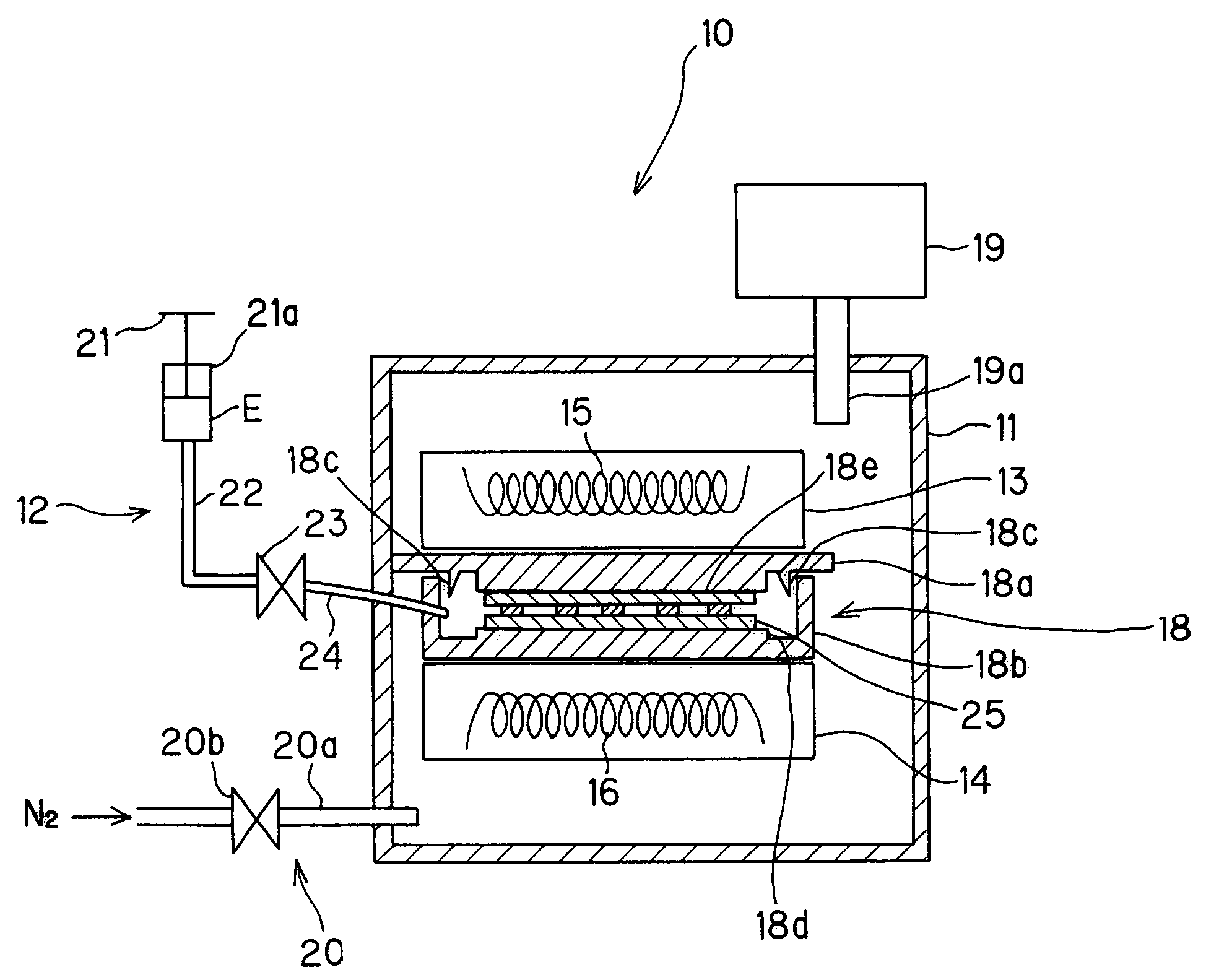
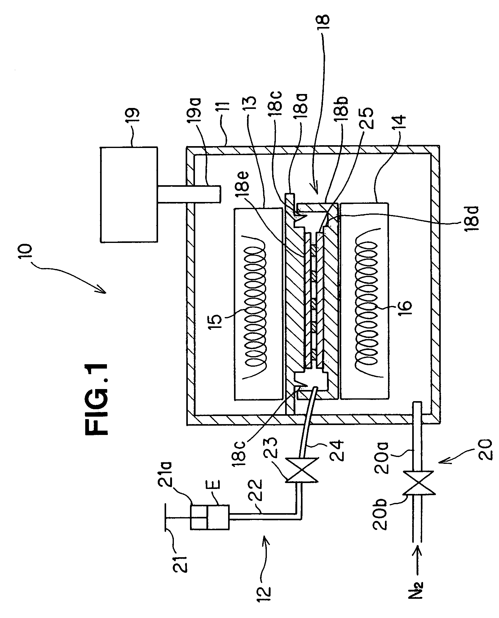
[0020]FIG. 1 is a sectional view of an adhesive injection apparatus in accordance with an embodiment of the present invention. The adhesive injection apparatus 10 includes: a vacuum chamber 11; an adhesive supply section 12; a receptacle 18 having upper and lower stages (fixing sections) 13 and 14, heating devices 15 and 16 and upper and lower jigs 18a and 18b; a pump or evacuation device 19; and an inert gas introduction section 20.

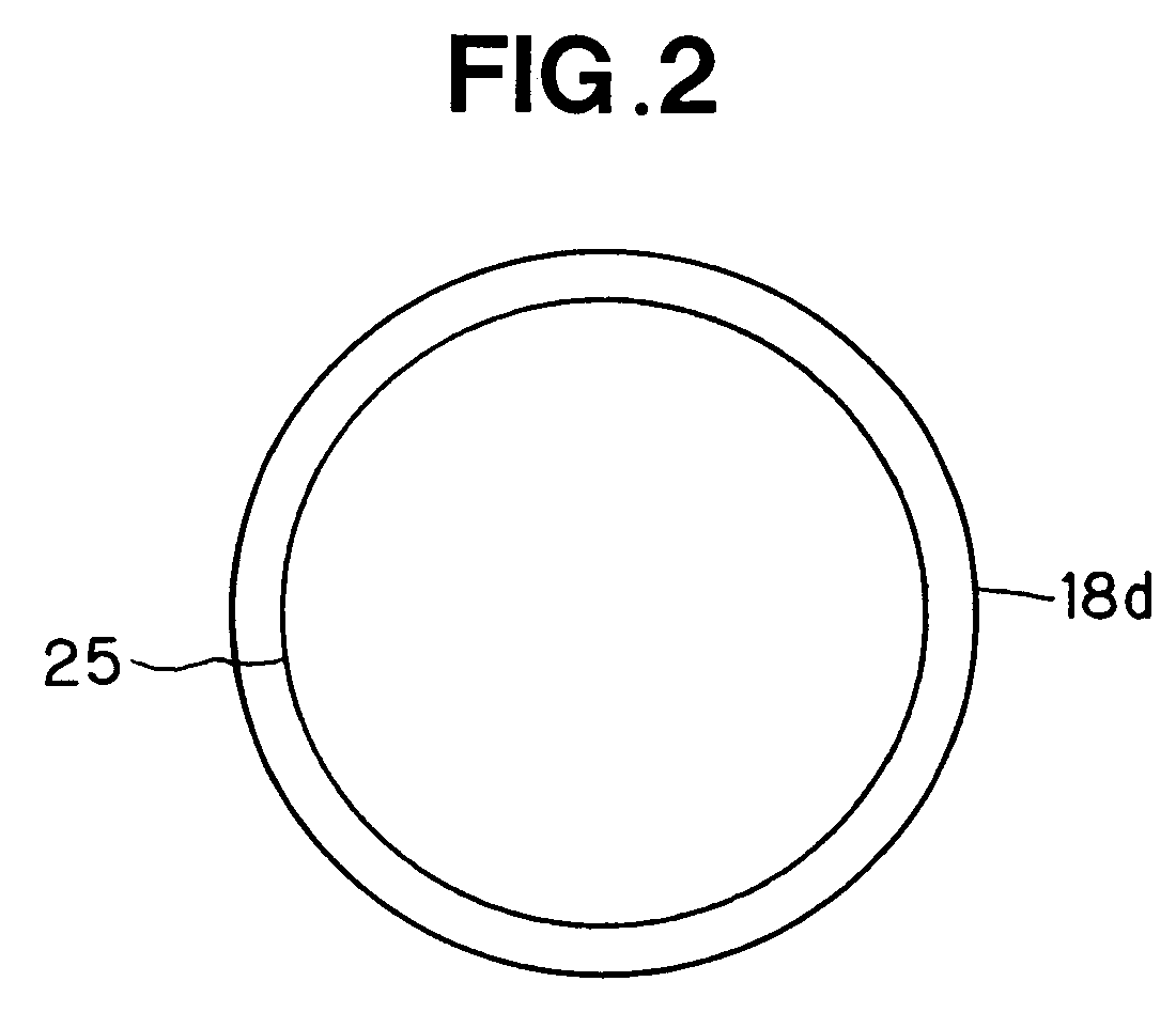
[0021]The adhesive supply section 12, which is a device for supplying an adhesive E in the form of liquid into the receptacle 18, includes a piston portion 21, supplying path 22, valve 23 and adhesive injecting portion 24. The adhesive E may be an epoxy-based adhesive, for example. The receptacle 18, including the upper and lower jigs 18a and 18b, is provided for receiving and loading (i.e., holding) therein a plurality of layers of stacked flat plate members 25, such as a plurality of layers of stacked wafers (collectively called “wafer stack”) 25 in a ...


PUM

PropertyMeasurementUnit
pressureaaaaaaaaaa
temperatureaaaaaaaaaa
surface areaaaaaaaaaaa

Abstract

Adhesive injection apparatus, designed to inject an adhesive into gaps between a plurality of layers of flat plate members, includes: a receptacle for holding therein the flat plate members; an evacuation section for evacuating the interior of the receptacle and the gaps between the flat plate members; an adhesive supply section for supplying the adhesive into the receptacle; and a gas introduction section for introducing a gas into the receptacle to produce a pressure difference between the interior of the receptacle and the gaps between the flat plate members, so as to allow the adhesive to be injected from all around the flat plate members into the gaps.

Description

FIELD OF THE INVENTION[0001]The present invention relates generally to adhesive injection apparatus and methods, and more particularly to an improved adhesive injection apparatus and method for use in manufacturing of three-dimensional semiconductor integrated circuit devices etc.BACKGROUND OF THE INVENTION[0002]Three-dimensional semiconductor integrated circuit devices have been known, in which two or more layers of wafers, each having a semi-conductor device or semiconductor integrated circuit device previously formed therein, are stacked vertically and the vertically-arranged semiconductor devices or semiconductor integrated circuit devices are electrically connected with each other via vertical wiring. For example, Japanese Patent Laid-Open Publication No. HEI-11-261001 discloses a method for manufacturing a three-dimensional semiconductor integrated circuit device, in accordance with which trenches (i.e., deep grooves) are formed in an upper-layer wafer having a semiconductor d...

Claims


Application Information

Patent Timeline
Patent Type & Authority Patents(United States)
IPC IPC(8): H01L21/56
CPCH01L21/67092H01L21/6715H01L2924/0002H01L2924/00
Inventor MIYAKAWA, NOBUAKITOSHIMA, HIROYUKINAKAMURA, NATSUOKIMURA, TAKAHIRO
Owner HONDA MOTOR CO LTD
Why Eureka
Try Eureka