Fabrication of semiconductor structure having N-channel channel-junction field-effect transistor

a field-effect transistor and semiconductor structure technology, applied in the field of semiconductor structure, can solve the problems of inability to control the operation of the igfet with the gate electrode, unsatisfactory terms, and the noise of the n-channel high-voltage scigfet b>80/b>, and achieve the effect of large noise reduction

Active Publication Date: 2009-09-29
NAT SEMICON CORP
View PDF20 Cites 116 Cited by
  • Summary
  • Abstract
  • Description
  • Claims
  • Application Information

AI Technical Summary

Benefits of technology

[0026]The present invention takes advantage of certain materials properties which are asymmetrical with respect to the n and p types of semiconductor conductivity to achieve an insulated-gate field-effect transistor technology having performance characteristics that are greatly improved over the prior art. These properties include (a) higher electron mobility than hole mobility, (b) higher electron channel-zone-to-gate-dielectric tunneling probability than hole channel-zone-to-gate-dielectric tunneling probability, and (c) differences in diffusion rates and other characteristics between n-type dopants and p-type dopants. By taking advantages of these materials properties, especially the electron-to-hole mobility difference and the electron-to-hole channel-zone-to-gate-dielectric tunneling probability difference, in accordance with the invention, the present IGFET technology enables 1 / f noise to be reduced by a large factor while signal gain is increased.
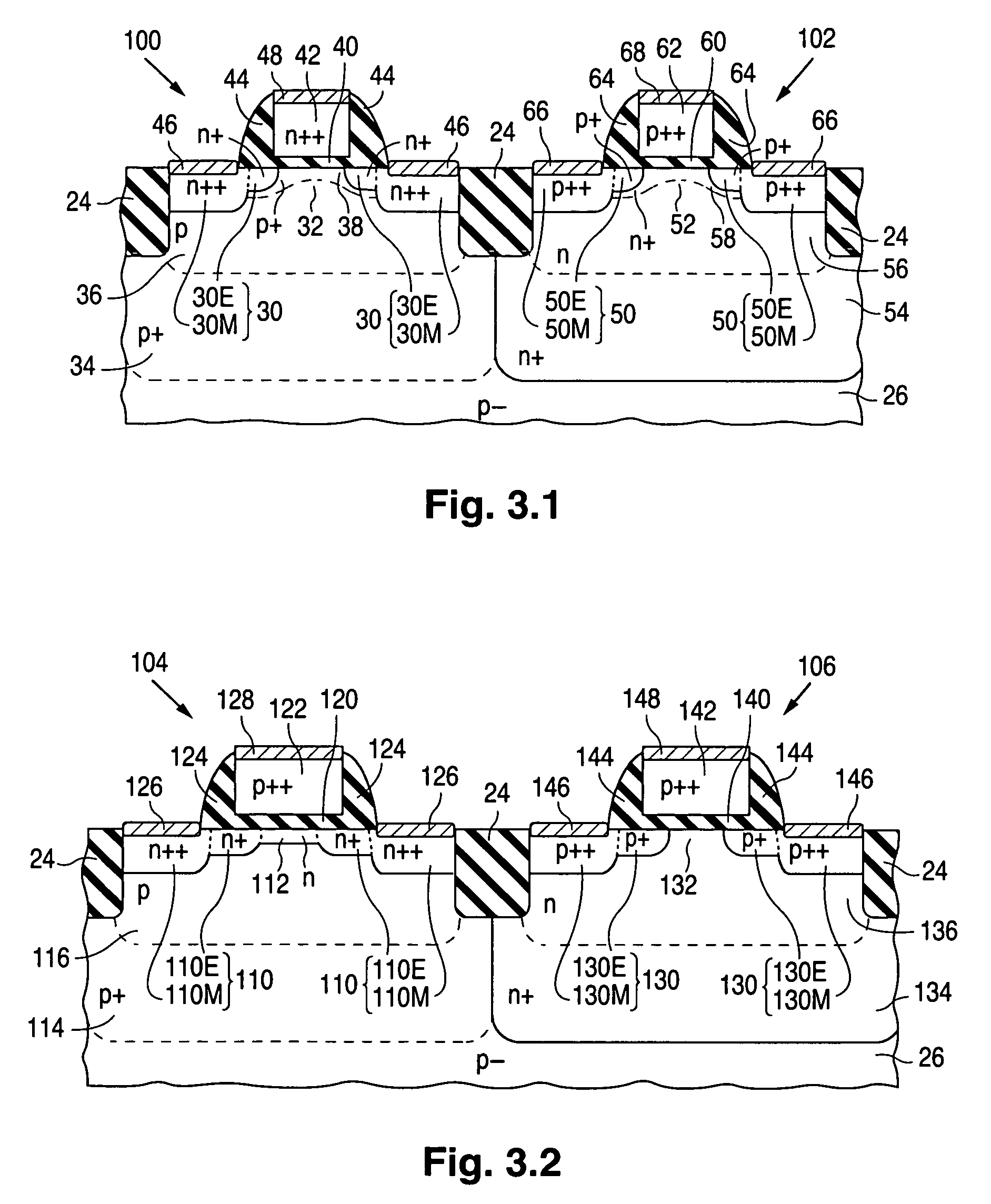
[0032]The IGFET processing in the foregoing alternative continues with the formation of a second dielectric layer, again preferably thicker than the first dielectric layer, along the semiconductor body at least along the lateral locations for the gate dielectric layers of the two SCIGFETs. A second semiconductor layer is formed over the second dielectric layer. The two semiconductor layers are then patterned and doped with suitable semiconductor dopants to define the gate electrodes for the three IGFETs. The gate dielectric layer of each SCIGFET again includes a portion of the second dielectric layer while the gate dielectric layer of the n-channel CJIGFET includes a portion of the remainder of the first dielectric layer. This alternative technique for defining the gate dielectric layers and gate electrodes, although slightly more complex than the first-mentioned technique, avoids exposing the material which later becomes the gate dielectric layer for the n-channel CJIGFET to potential contaminates, such as photoresist employed in removing largely all the material of the first dielectric layer along the lateral locations for the gate dielectric layers of the two SCIGFETs, since the first semiconductor layer covers the first dielectric layer at that point in the alternative technique.
[0038]In short, the present invention achieves a very large noise reduction. Fabrication of the complementary-IGFET structure of the invention is straightforward and does not require complicated processing steps. Accordingly, the invention provides a large advance over the prior art.

Problems solved by technology

If the drain depletion region punches through to the source depletion region, the operation of the IGFET cannot be controlled with the gate electrode.
Unfortunately, all of these terms are unsatisfactory.
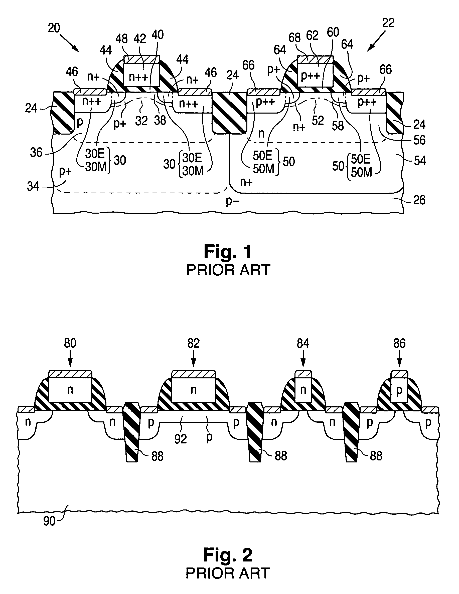
Unfortunately, n-channel high-voltage SCIGFET 80 appears to be relatively noisy.

Method used


Image

  • Fabrication of semiconductor structure having N-channel channel-junction field-effect transistor
  • Fabrication of semiconductor structure having N-channel channel-junction field-effect transistor
  • Fabrication of semiconductor structure having N-channel channel-junction field-effect transistor

Examples


Embodiment Construction

Reference Notation and Other Conventions

[0051]The reference symbols employed below and in the drawings have the following meanings:

[0052]

CGD ≡gate dielectric capacitance per unit areaDOSENPOLY ≡areal dosage of ions of n-type polysilicon gate-electrodedopantDOSEPPOLY ≡areal dosage of ions of p-type polysilicon gate-electrodedopantEGD ≡transversal electric field in gate dielectric layerEST ≡transversal electric field at surface of channel zone atthreshold conditionf ≡frequencyh ≡Planck's constantL ≡channel length along upper semiconductor surfacem0 ≡free electron massm* ≡density-of-states effective mass of charge carriers in gatedielectric layerM ≡empirical parameterMA ≡number of azimuthal anglesn ≡non-ideality factorNB ≡uniform net dopant concentration in body materialNB0 ≡background dopant concentration in body materialNC ≡uniform net dopant concentration in channel zoneNC0 ≡net dopant concentration at upper surface of channel zoneNN ≡local net dopant concentrationNNPOLY ≡uniform ne...


PUM


Abstract

A semiconductor technology combines a normally off n-channel channel-junction insulated-gate field-effect transistor (“IGFET”) (104) and an n-channel surface-channel IGFET (100 or 160) to reduce low-frequency 1 / f noise. The channel-junction IGFET is normally fabricated to be of materially greater gate dielectric thickness than the surface-channel IGFET so as to operate across a greater voltage range than the surface-channel IGFET. A p-channel surface-channel IGFET (102 or 162), which is typically fabricated to be of approximately the same gate-dielectric thickness as the n-channel surface-channel IGFET, is preferably combined with the two n-channel IGFETs to produce a complementary-IGFET structure. A further p-channel IGFET (106, 180, 184, or 192), which is typically fabricated to be of approximately the same gate dielectric thickness as the n-channel channel-junction IGFET, is also preferably included. The further p-channel IGFET can be a surface-channel or channel-junction device.

Description

CROSS-REFERENCE TO RELATED APPLICATION[0001]This is a division of U.S. patent application Ser. No. 10 / 803,203, filed 17 Mar. 2004, now U.S. Pat. No. 7,176,530 B1.FIELD OF USE[0002]This invention relates to semiconductor technology and, in particular, to field-effect transistors of the insulated-gate type.BACKGROUND ART[0003]An insulated-gate field-effect transistor (“IGFET”) is a semiconductor device in which a gate dielectric layer electrically insulates a channel zone of a semiconductor body from an overlying gate electrode. The channel zone extends between a source and a drain that adjoin a body region of the semiconductor body. The body region, often referred to as the substrate region or substrate, is of opposite conductivity type to the source and drain. Charge carriers, i.e., electrons for an n-channel IGFET and holes for a p-channel IGFET, move from the source through the channel zone to the drain when appropriate voltages are applied to the gate electrode, source, drain, an...

Claims


Application Information

Patent Timeline
Patent Type & Authority Patents(United States)
IPC IPC(8): H01L21/8236
CPCH01L21/823807H01L27/0883H01L29/7833H01L29/1041H01L29/105H01L27/0928H01L21/26586H01L29/665
Inventor BULUCEA, CONSTANTINLINDORFER, PHILIPP
Owner NAT SEMICON CORP
Why Eureka
Try Eureka