

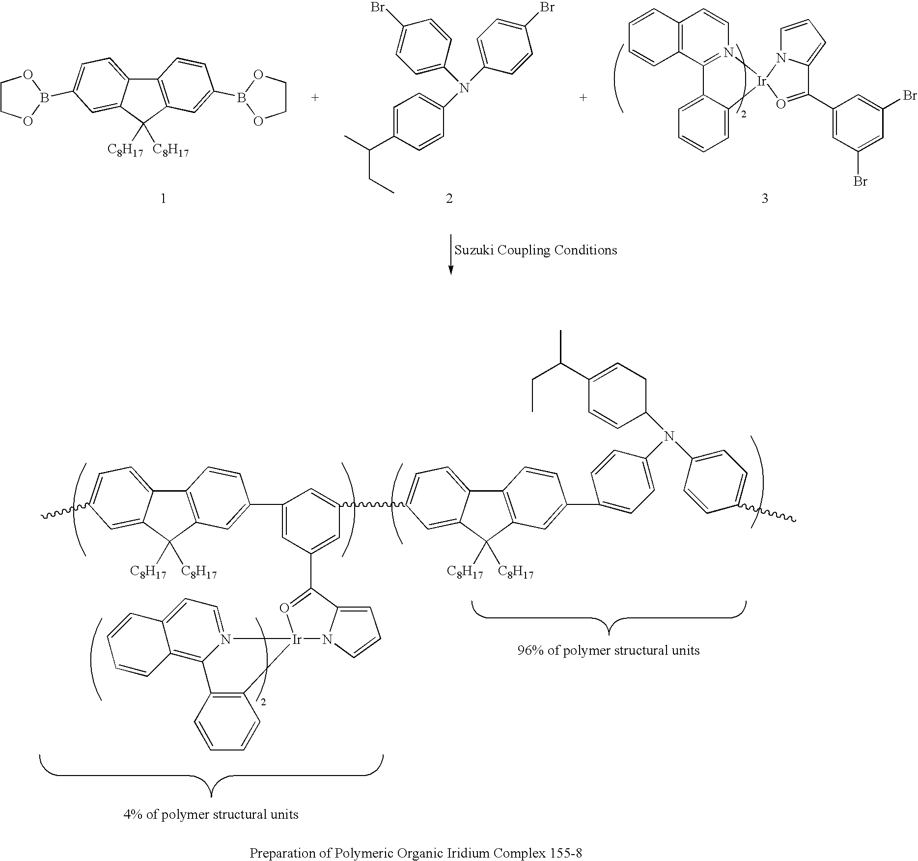
Method of making organic light emitting devices
a light-emitting device and organic technology, applied in thermoelectric devices, solid-state devices, transportation and packaging, etc., can solve the problems of difficult to achieve continuous and coalesced film coverage, difficult to fabricate a multi-layered device comprising organic materials, and inability to heat light-emitting materials used in oleds
- Summary
- Abstract
- Description
- Claims
- Application Information
AI Technical Summary
Benefits of technology
Problems solved by technology
Method used
Image

Examples
examples 3-11
[0073]In another series of experiments (See Table III) the effect of the structure of the INP precursor material on relative fluorescence quantum yield and the robustness of the film comprising the interpenetrating network polymer composition, as measured by post-cure film solubility, was investigated. Films comprising an electroluminescent polymer, BP79, and an INP precursor material (NORLAND 68 OPTICAL ADHESIVE (“N-68”) or SR-454) were prepared as described in the General Methods section. Each film was subjected to UV curing under an atmosphere of nitrogen. Film compositions, cure times, relative fluorescence quantum yields, and solubility data are presented in Table III below.
TABLE IIIINPWt. % INPUV CurePost-cureprecursorprecursorTimefilmEntrymaterialmaterial*(minutes)QErelsolubiltyExample-3N-6815150.59453Example-4N-681530.62242Example-5N-6830150.70622Example-6N-683030.70615Example-7N-685150.83285Example-8SR-4545150.71085Example-9SR-45415150.86129Example-SR-45430150.8351210Exampl...
examples 24-29
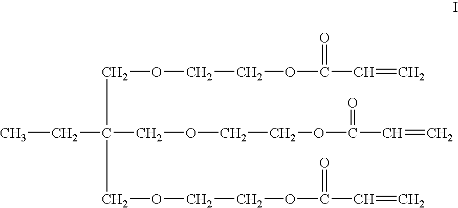
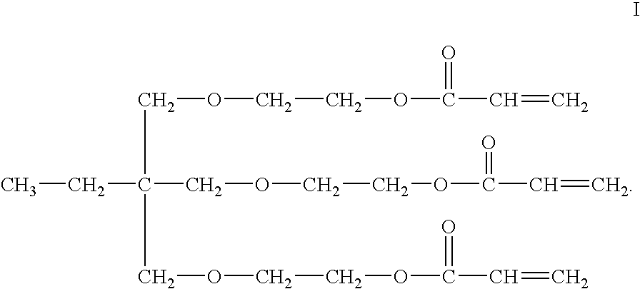
[0081]Cured films were prepared as described in the General Methods section from combinations of one or more of five INP precursor materials with an electroactive polymer selected from BP79 and ADS145UV. For films comprising BP79, curing was carried out using a Blak-Ray UVL-56 UV lamp with an intensity of 3.8 mW / cm2 at 365 nm. Exposure time was 15 minutes. For films comprising ADS145UV, curing was carried out using a unfiltered UVP model R-52G 254 nm source UV lamp (estimated intensity of ˜25 mW / cm2 at 254 nm) and the exposure time was 1 minute. In each of Examples 24-29, the weight percentage of the INP precursor material in the uncured films was about 30% and the weight percentage of the electroactive polymer was about 70 percent. As noted, “SR295” is pentaerythritol tetraacrylate; “SR368D” is tris(2-hydroxyethyl) isocyanurate triacrylate; “SR454” is ethoxylated (3 mole) trimethylolpropane triacrylate; “SR502” is ethoxylated (9) trimethylolpropane triacrylate; and “CN975” is a hex...
example 30
[0082]Preparation Of An OLED Device Fabricated According To The Method Of The Present Invention: A layer of PEDOT / PSS (Baytron P VP 8000, a poly(3,4-ethylenedioxythiophene)-poly(styrenesulfonate) obtained as a solution from HC Starck, Inc.) having a thickness of about 60 nm was deposited by spin-coating onto clean, UV-Ozone treated, 2.5 cm×2.5 cm ITO patterned glass substrates. The coated substrates were then baked on a hot plate in air for 30 minutes at 160° C. A layer of F8-TFB (an octylfluorene-triarylamine copolymer obtained from Sumation, Inc.) hole transporter layer having a thickness of about 10-20 nm was then spin-coated atop the PEDOT / PSS coated substrates. The F8-TFB-PEDOT / PSS coated substrates were then baked on a hot plate in argon for 30 minutes at 160° C. A layer comprised of the electroluminescent polymer BP79 blended with the INP precursor material SR454 acrylate (obtained from Sartomer, Inc.) was then spin-coated from a xylene solution atop the F8-TFB layer. The wei...
PUM
| Property | Measurement | Unit |
|---|---|---|
| temperatures | aaaaa | aaaaa |
| wavelengths | aaaaa | aaaaa |
| wavelength range | aaaaa | aaaaa |
Abstract
Description
Claims
Application Information