

Charged particle beam writing method and apparatus
a writing method and charge technology, applied in the field of charged particle beam writing method and charged particle beam writing apparatus, can solve the problems of system limitations and difficulty in further and achieve the effect of shortening the writing tim
- Summary
- Abstract
- Description
- Claims
- Application Information
AI Technical Summary
Benefits of technology
Problems solved by technology
Method used
Image

Examples
first embodiment
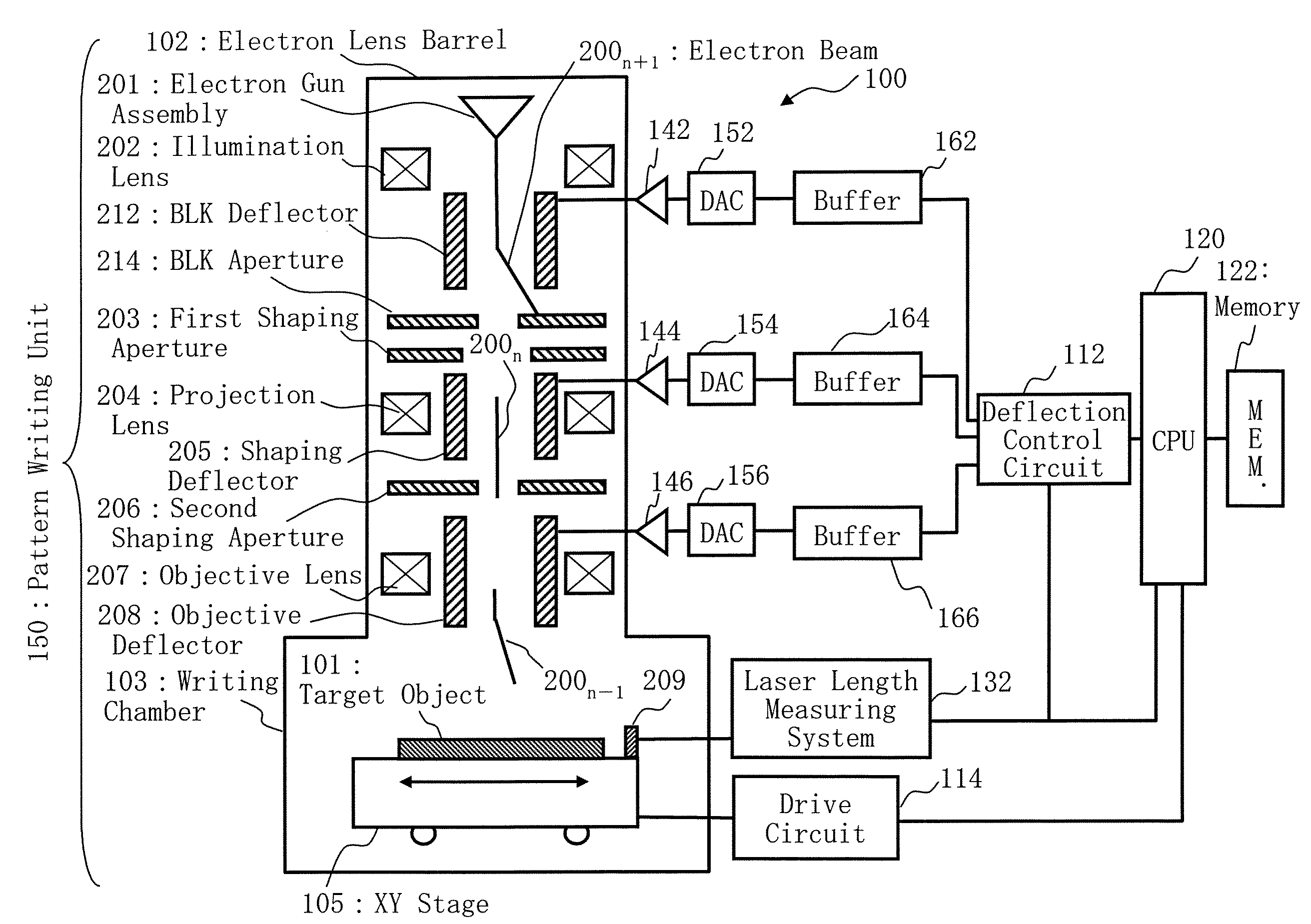
[0030]FIG. 1 is a conceptual diagram showing a configuration of a writing apparatus according to a first embodiment.
[0031]FIG. 1 shows, as an example of a charged particle beam writing apparatus, a writing apparatus 100 serving as a variable-shaped electron beam writing apparatus. The writing apparatus 100 writes, or “draws” a pattern on a target object 101. The writing apparatus 100 includes a pattern writing unit 150 and a control system. The pattern writing unit 150 includes an electron lens barrel 102, a writing chamber 103, an X-Y stage 105, an electron gun assembly 201, an illumination lens 202, a blanking (BLK) deflector 212, a BLK aperture 214, a first shaping aperture 203, a projection lens 204, a shaping deflector 205, a second shaping aperture 206, an objective lens 207, an objective deflector, or “position deflector”208, and a reflecting mirror 209. The control system includes a control computer (CPU) 120 serving as a computer, a memory 122, a deflection control circuit ...
second embodiment
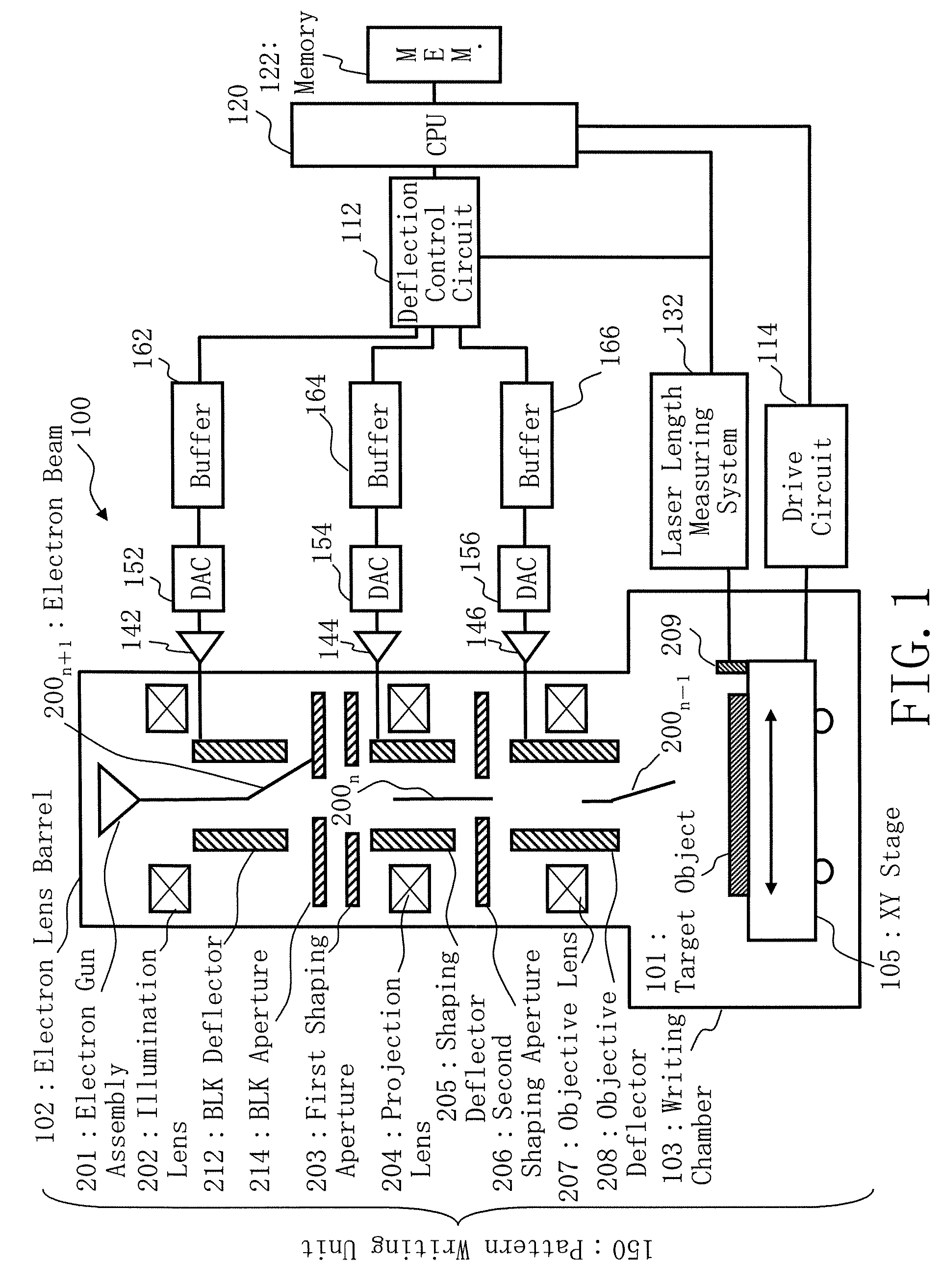
[0061]FIG. 7 is a conceptual diagram showing a configuration of a writing apparatus according to a second embodiment.
[0062]FIG. 7 is the same as FIG. 1 except that a buffer memory 172, 174, and 176 are arranged in a deflection control circuit 112. In FIG. 7, a distribution circuit 180 which is omitted in FIG. 1 is shown. The DAC 152 is connected to the buffer memory 172. Similarly, the DAC 154 is connected to the buffer memory 174. Similarly, the DAC 156 is connected to the buffer memory 176. In the first embodiment, the respective buffer memories are arranged on respective deflector sides serving as receiving sides of output signals from the deflection control circuit 112. However, the second embodiment is the same as the first embodiment except that the buffer memories are arranged in the deflection control circuit 112 and arranged on sending sides to the deflectors. In FIG. 7, constituent elements required for explaining the second embodiment are described. In general, a writing ...
third embodiment
[0065]FIG. 8 is a conceptual diagram showing a configuration of a writing apparatus according to a third embodiment.
[0066]In FIG. 8, a writing apparatus 100 includes, as an example of a pattern writing unit 150, an electron lens barrel 102, a writing chamber 103, an X-Y stage 105, an electron gun assembly 201, an illumination lens 202, a first BLK deflector 221, a second BLK deflector 222, a BLK aperture 214, a first shaping aperture 203, a projection lens 204, a first shaping deflector 224, a second shaping deflector 225, a second shaping aperture 206, an objective lens 207, a first objective deflector 226, a second objective deflector 228, and a reflecting mirror 209. The writing apparatus 100 includes, as a control system, a CPU 120, a memory 122, a deflection control circuit 112, a laser length measuring system 132, a drive circuit 114, a deflecting amplifier 142, a DAC 152, a buffer memory 162, a deflecting amplifier 143, a DAC 153, a buffer memory 163, a deflecting amplifier 1...
PUM
 Abstract
Description
Claims
Application Information