
Calibrating a phase detector and analog-to-digital converter offset and gain

a phase detector and analog-to-digital converter technology, applied in the field of data communication circuits, can solve the problems of large phase offset, unsatisfactory jitter tolerance bandwidth, and large phase offset, so as to reduce or eliminate the offset of phase detectors, reduce the gain errors of phase detectors and adcs

Active Publication Date: 2009-10-27
SKYWORKS SOLUTIONS INC
View PDF10 Cites 3 Cited by
  • Summary
  • Abstract
  • Description
  • Claims
  • Application Information

AI Technical Summary

Benefits of technology

The present invention provides apparatus and methods for reducing errors and offsets in a phase detector and an ADC. This is achieved by generating an error pulse and a reference pulse, combining them into a phase detector pulse, and using an ADC that has its full scale set by an average of the reference pulse. Additionally, a calibration loop is used to generate a phase adjust value to force a filtered value of the ADC output to substantially zero, which can then be stored and used during normal operation to reduce or remove phase offsets. The invention can be implemented in hardware, firmware, or software, and may include additional components such as an amplifier to convert incoming optical energy into voltage signals.

Problems solved by technology

However, such phase detectors rely on the matching of delays between data and clock paths.
Accordingly, these phase detectors are notorious for having large phase offsets that change with process.
However, the I / C ratio does not track well from silicon wafer to silicon wafer.
Such gain variations cause jitter transfer and jitter tolerance bandwidths to undesirably vary.
However, it is very difficult to match this delay to the clock-to-Q delay of the latch.
These unmatched delays cause non-optimal phase sampling due to offsets in the phase detector.

Method used


Image

  • Calibrating a phase detector and analog-to-digital converter offset and gain
  • Calibrating a phase detector and analog-to-digital converter offset and gain
  • Calibrating a phase detector and analog-to-digital converter offset and gain

Examples


Embodiment Construction

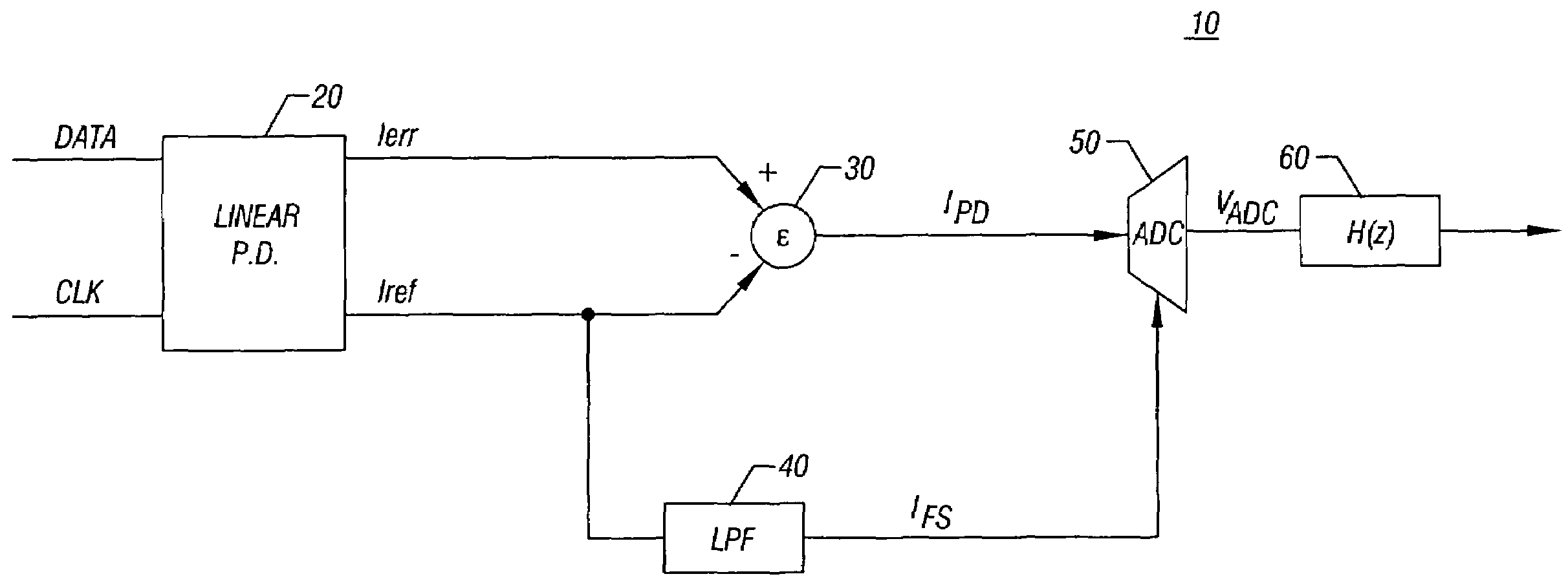
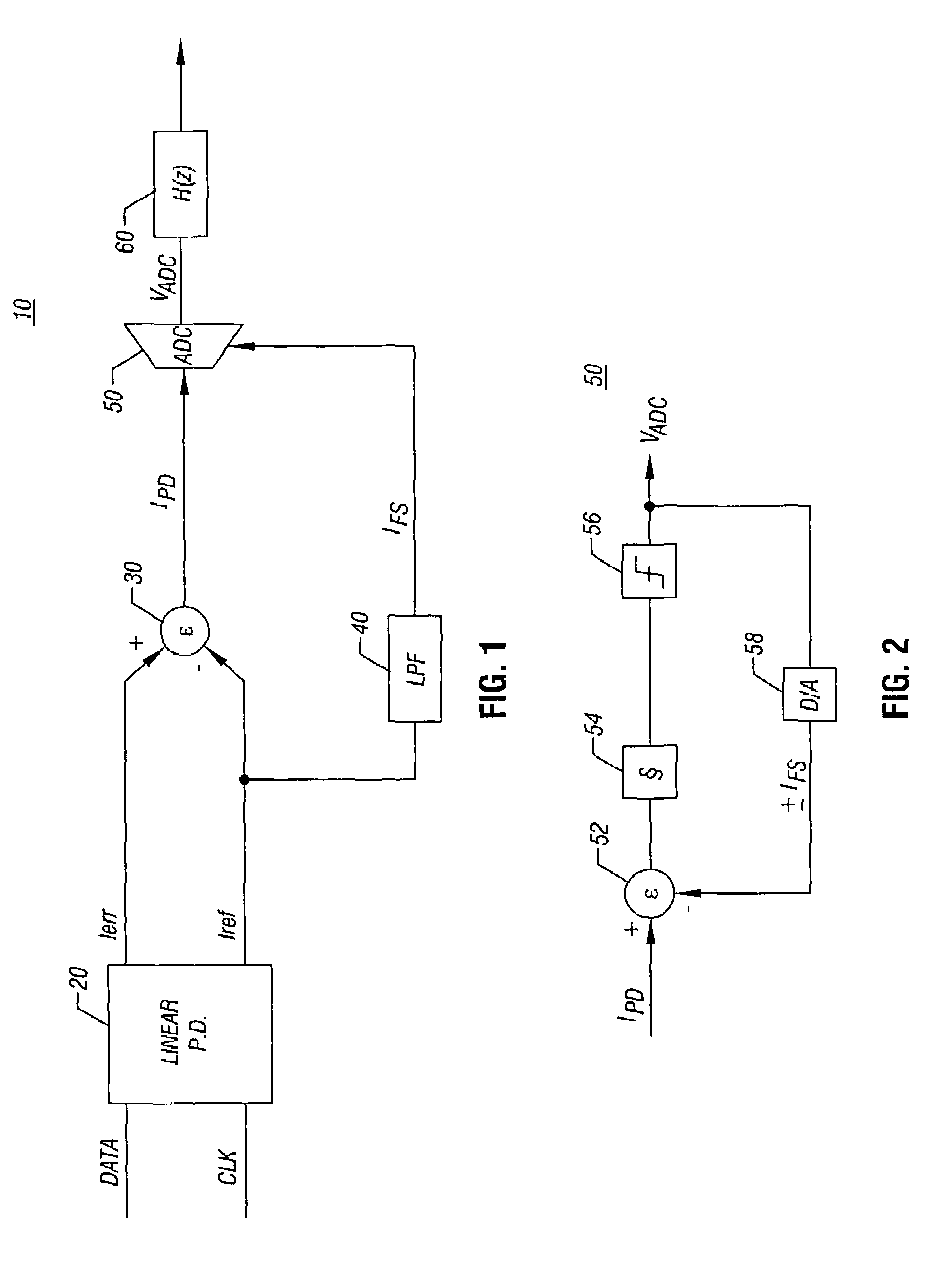
[0019]Referring to FIG. 1, shown is a block diagram of a portion of a clock and data recovery (CDR) circuit in accordance with one embodiment of the present invention. More specifically, FIG. 1 shows a phase detector and a related analog-to-digital converter (ADC) and digital filter to generate a control voltage (e.g., a voltage controlled oscillator (VCO) control voltage) from an incoming data path.

[0020]As shown in FIG. 1, circuit 10 includes a linear phase detector 20, which receives incoming data and a clock signal. In one embodiment, the incoming data may be received from a limit amplifier (LA) or an automatic gain control (AGC) amplifier, which may be within an integrated circuit (IC) package including a CDR. While not shown in FIG. 1, the clock signal (CLK) may be generated in the CDR from the incoming data and be fed back to phase detector 20.

[0021]Phase detector 20 may be a high-speed linear phase detector having an error output and a reference output. More specifically, ph...


PUM


Abstract

The present invention includes apparatus and methods to calibrate a phase detector and an analog-to-digital converter (ADC) offset and gain. In one such embodiment, an apparatus includes a phase detector to generate an error pulse and a reference pulse, a combiner to combine the pulses, and an ADC to receive the combined pulses, where the ADC has a full scale set by an average of the reference pulse. Still further, a calibration loop may be coupled between the output of the ADC and the phase detector to generate and provide a phase adjust signal to reduce or eliminate phase offsets. Other embodiments are described and claimed.

Description

FIELD OF THE INVENTION[0001]The present invention relates to data communication circuits, and more specifically to such circuits including a phase detector.BACKGROUND[0002]Communication systems often transmit data with a clock embedded in a data stream, rather than being sent as a separate signal. When the data stream is received, a clock and data recovery circuit (CDR) recovers the embedded clock and retimes the received data to the recovered clock. Typically, a phase-locked loop (PLL) is used to perform the clock recovery operation. Such a PLL typically includes a phase detector, which receives the input data signal and a clock signal from a voltage-controlled oscillator (VCO). The phase detector generates an error signal, which is a function of the phase difference between the input data signal and the VCO clock signal. The phase detector may also include additional circuitry to generate the reconstructed data.[0003]The phase detector, oftentimes a linear phase detector, is used ...

Claims


Application Information

Patent Timeline
Patent Type & Authority Patents(United States)
IPC IPC(8): H04L25/00
CPCH04L7/033H04L7/0004
Inventor ELDREDGE, ADAM B.BATCHELOR, JEFFREY S.HAMMES, GARY
Owner SKYWORKS SOLUTIONS INC
Learn More