Method for manufacturing a semiconductor device and semiconductor device

a manufacturing method and technology for semiconductor devices, applied in semiconductor devices, semiconductor/solid-state device details, electrical devices, etc., can solve the problems of conductive layer b>18/b> being liable to come off or separate, increasing wiring resistance, and burdening the process, so as to facilitate reaction, increase metal segregation sites, and surface roughness of insulating films at a sid

Active Publication Date: 2009-11-03
SONY CORP
View PDF6 Cites 12 Cited by
  • Summary
  • Abstract
  • Description
  • Claims
  • Application Information

AI Technical Summary

Benefits of technology

[0018]According to the first manufacturing method of a semiconductor device and the first semiconductor device thus obtained, since at least a part of the insulating film constituting the inner wall side of the recess is porositized, the porous portion is lower in density than the non-porous insulating film, by increasing a surface roughness at the inner walls of the recess. In doing so, when the thermal treatment is carried out in the fourth step wherein the metal in the alloy layer is reacted with a constituent component in the insulating film, a segregation site for the metal in the alloy layer increases in number. This facilitates the above reaction by promoting the formation of a self-formed barrier film at the interface between the alloy layer and the insulating film. The porous portion is likely to absorb moisture, and oxygen is supplied from the moisture at the interface between the alloy layer and the insulating film, so that the reaction between the metal in the alloy layer and the constituent component of the insulating film is facilitated, by promoting the formation of the self-formed barrier film.
[0021]According to the second manufacturing method of a semiconductor device and the second semiconductor device thus obtained, since the modified layer whose density is lower than the insulating film is formed at an inner wall side of the recess, the surface roughness of the insulating film at a side of the inner walls of the recess increases. This, in turn, increases metal segregation sites on or in the alloy layer when thermal treatment is carried out at the fifth step in order to cause the metal in the alloy layer to react with the constituent component of the insulating film. Consequently, the reaction is facilitated and the formation of the self-formed modified layer at the interface between the alloy layer and the modified layer is also facilitated. Additionally, the modified layer is likely to absorb moisture, and oxygen is supplied from the moisture at the interface between the alloy layer and the modified layer, by facilitating the reaction between the metal in the alloy layer and the constituent component of the modified layer to promote the formation of the self-formed barrier film.
[0022]As stated hereinabove, according to the manufacturing method of a semiconductor device and the semiconductor device of an embodiment of the present invention, the formation of the self-formed barrier film at the interface between the alloy layer and the insulating layer is facilitated, for which a continuous self-formed barrier layer is likely to be formed at an initial stage of the thermal treatment. This leads to improved adhesion between the conductive layer and the insulating layer, thus enabling the conductive layer to be prevented from separation. Hence, the yield of the semiconductor device can be improved.

Problems solved by technology

In a subsequent CMP step, the conductive layer 18 receives a lateral stress by the polishing, with a problem that the conductive layer 18 is liable to come off or separate.
Since Mn is higher in resistance than Cu, there arise problems in that not only a wiring resistance increases if Mn remains in the wiring, but also the sheet resistance of the alloy layer 17 increases, so that a load is burdened on the process wherein the conductive layer is buried by the plating method.

Method used


Image

  • Method for manufacturing a semiconductor device and semiconductor device
  • Method for manufacturing a semiconductor device and semiconductor device
  • Method for manufacturing a semiconductor device and semiconductor device

Examples


first embodiment

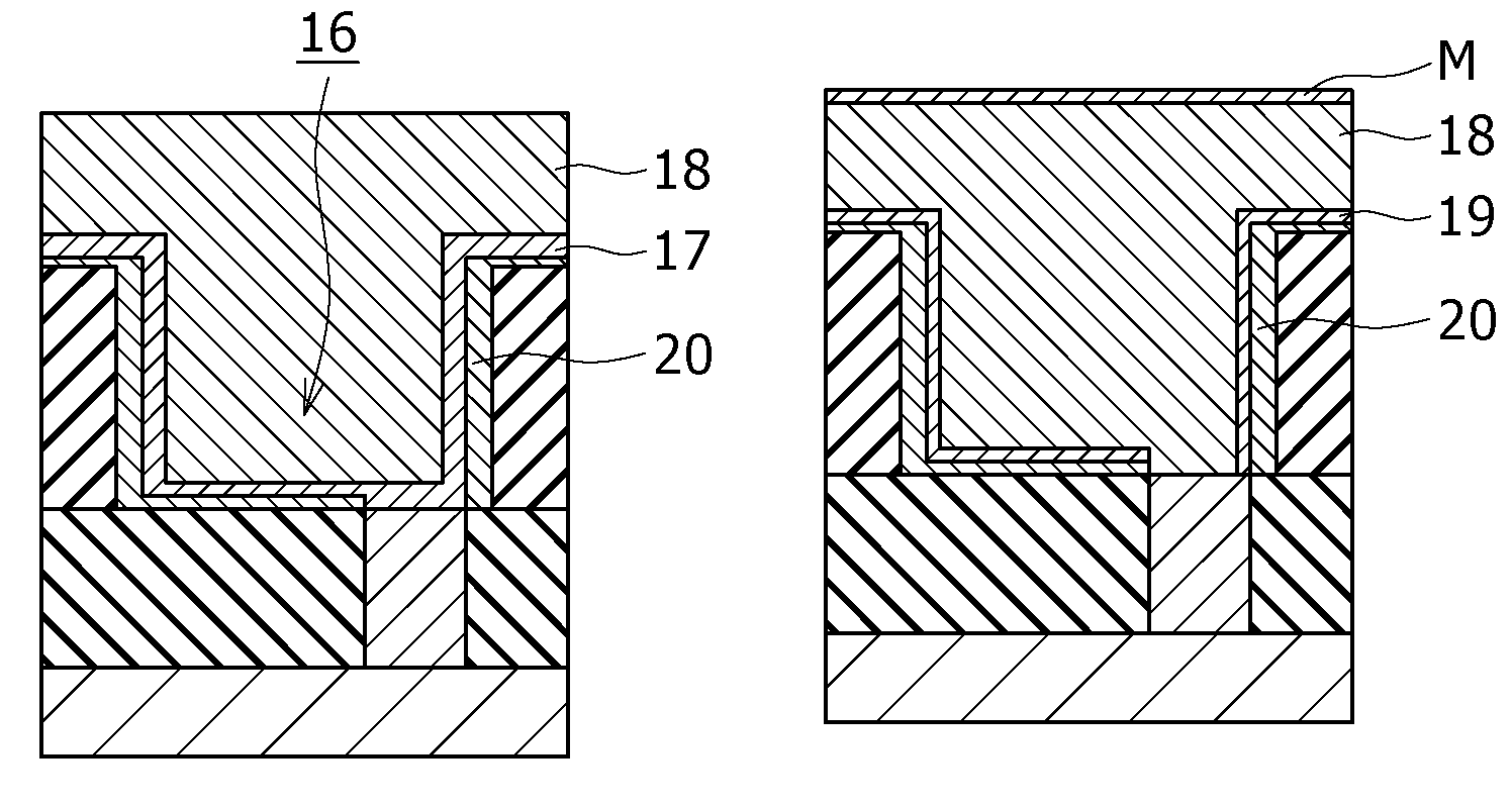
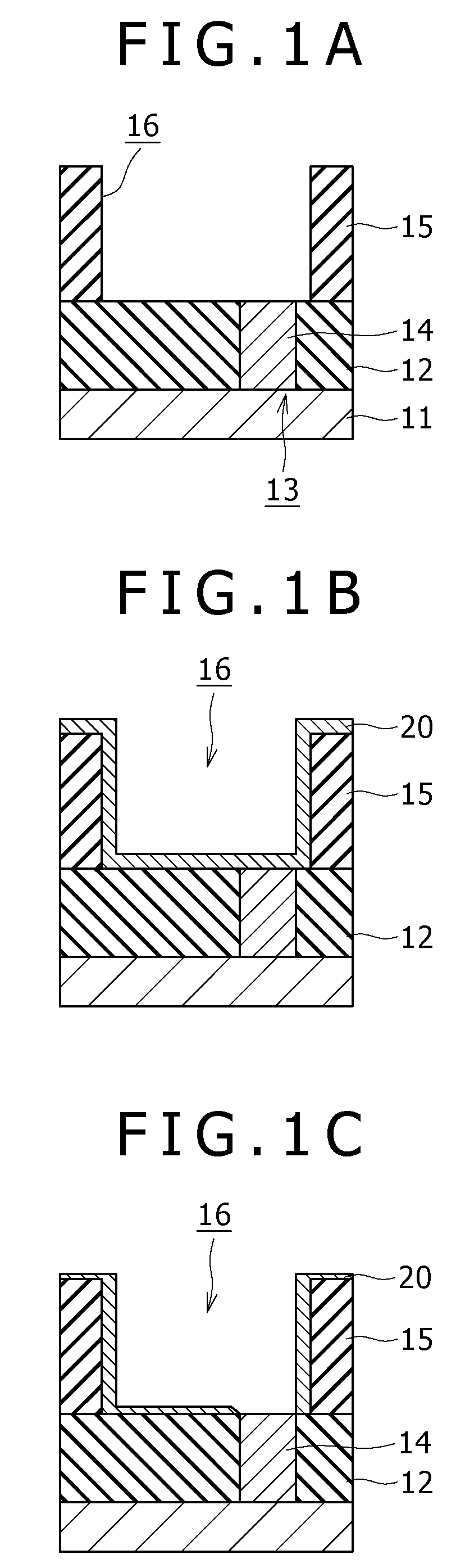
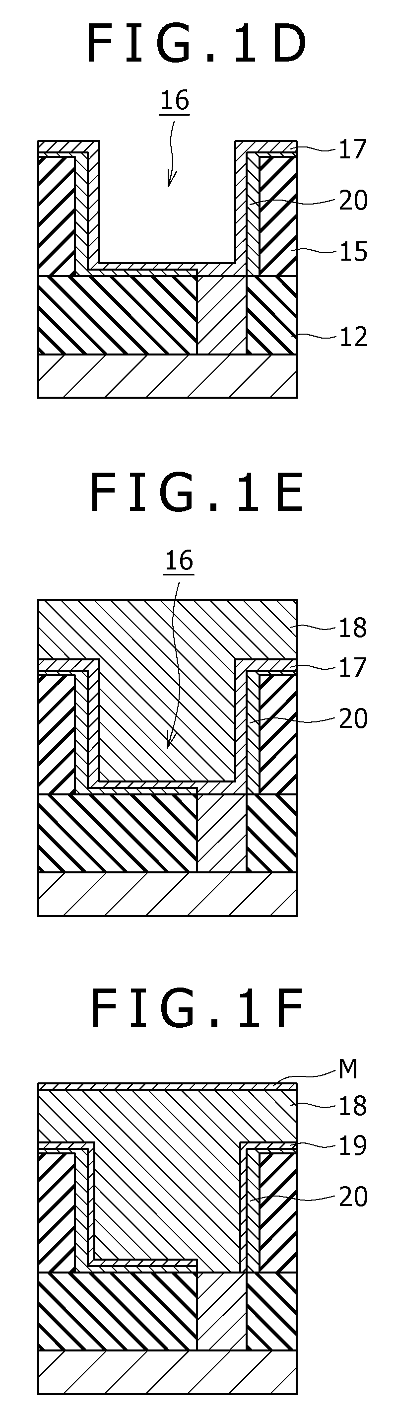
[0032]This embodiment is an example embodying a manufacturing method of a semiconductor device according to an embodiment of the present invention and relates to formation of a single damascene wiring structure. A first embodiment of the invention is illustrated with reference to the sectional views of FIGS. 1A to 1F showing manufacturing steps, respectively. It is to be noted that like members or parts as in Description of the Related Art are indicated by like reference symbols.

[0033]As shown in FIG. 1A, a non-porous interlayer insulating film 12 made, for example, of SiO2 is formed on a substrate 11 constituted of a silicon wafer in which an element such as a transistor has been formed. Thereafter, a contact hole 13 arriving at the substrate 11 is formed and a via 14 made, for example, of W is formed as buried in the contact hole 13.

[0034]Next, a non-porous interlayer insulating film 15 made, for example, of SiO2 is formed in a thickness of 500 nm on the interlayer insulating film...

modification 1

(Modification 1)

[0056]Although the porous film 20 has been formed herein so as to cover the inner walls of the wiring groove 16 so that the wiring groove 16 is rendered porous at the inner wall side thereof to make a low density portion as is shown in FIG. 1B, the wiring groove 16 may be rendered low in density at a side of the inner walls thereof according to the following procedure.

[0057]As shown in FIG. 4A, a wiring groove 16 arriving at an interlayer insulating film 12 and a via 14 is formed in an interlayer insulating film 15. Next, the interlayer insulating films 12, 15 provided in the wiring groove 16 are subjected to plasma treatment, so that a modified layer 22 whose density is lower than the interlayer insulating films 12, 15 is formed at the inner wall side of the wiring groove 16. This modified layer 22 is increased in surface roughness over the non-porous interlayer insulating films 12, 15, for which when an alloy layer made of CuMn is formed on the modified layer 22 in...

second embodiment

[0067]A second embodiment relating to a manufacturing method of a semiconductor device according to an embodiment of the present invention is illustrated with reference to FIGS. 5A to 5L, each showing, in section, a manufacturing step of a semiconductor device. An instance of forming a dual damascene structure on the cap film illustrated with reference to FIG. 2 in the first embodiment is now described.

[0068]Initially, as shown in FIG. 5A, an interlayer insulating film 23 made, for example, of SiO2 is formed on the cap film 21, for example, by a PE-CVD method in a thickness of 700 nm. Although assuming herein that the interlayer insulating film 23 is formed of a single-layer film of SiO2, the interlayer insulating film 23 may have a hybrid structure wherein an organic insulating layer and an inorganic insulating layer are laminated.

[0069]Subsequently, a resist pattern (not shown) having a contact hole pattern is formed over the interlayer insulating film 23 and a contact hole 24a ar...


PUM

PropertyMeasurementUnit
densityaaaaaaaaaa
thicknessaaaaaaaaaa
thicknessaaaaaaaaaa

Abstract

A method for manufacturing a semiconductor device includes: the first step of forming, in an insulating film provided on a substrate, a recess that is porositized at least at inner walls; the second step of forming an alloy layer made of copper and a metal other than copper so as to cover the inner walls of the recess; the third step of burying a conductive layer made primarily of copper in the recess provided with the alloy layer; the fourth step of subjecting the thus treated substrate to thermal treatment to cause the metal in the alloy layer to react with a constituent component of the insulating film to form a barrier film made of a metal compound having Cu diffusion barrier properties.

Description

CROSS REFERENCES TO RELATED APPLICATIONS[0001]The present invention contains subject matter related to Japanese Patent Application JP 2006-241039 filed with the Japan Patent Office on Sep. 6, 2006, the entire contents of which being incorporated herein by reference.BACKGROUND OF THE INVENTION[0002]1. Field of the Invention[0003]This invention relates to a method for manufacturing a semiconductor device and also to a semiconductor device. More particularly, the invention relates to a method for manufacturing a semiconductor device having a damascene structure wherein a self-formed barrier film is provided between a wiring or via and an interlayer insulating film and also to such a semiconductor device.[0004]2. Description of the Related Art[0005]In copper (Cu) wiring formation process of a semiconductor device, it is general to use a damascene method wherein a wiring pattern is formed by burying a wiring groove formed in an interlayer insulating film. For the formation of Cu wiring a...

Claims


Application Information

Patent Timeline
Patent Type & Authority Patents(United States)
IPC IPC(8): H01L23/52
CPCH01L21/76826H01L21/76831H01L21/76844H01L23/53295H01L21/76867H01L21/76873H01L23/53238H01L21/76864H01L21/76835H01L2924/0002H01L2924/00H01L21/28
Inventor OHBA, YOSHIYUKIHAYASHI, TOSHIHIKO
Owner SONY CORP
Why Eureka
Try Eureka