Double-masking technique for increasing fabrication yield in superconducting electronics

a superconducting electronic and double-masking technology, applied in the direction of superconducting devices, originals for photomechanical treatment, instruments, etc., can solve problems such as major fabrication defects, achieve the effects of improving reliability and ic yield, increasing the number of steps, and improving ic yield

Active Publication Date: 2009-11-10
SEEQC INC
View PDF9 Cites 12 Cited by
  • Summary
  • Abstract
  • Description
  • Claims
  • Application Information

AI Technical Summary

Benefits of technology

[0013]The invention recognizes that failure of interlayer adhesion between photoresist and Nb is a major cause of defects in the fabrication technology of the prior art. By substantially improving such adhesion, the present invention offers the possibility of improved reliability and IC yield.
[0014]In the prior art, the very same photoresist mask had to survive two subsequent fabrication steps—etching and self-aligned junction anodization (passivation) without loss of adhesion. The new technique is more robust in this respect since the bottom layer of the double-layer would prevent defect formation during anodization even if the top (resist) layer fails. This technique has been incorporated into a complete IC process, and indeed has resulted in substantially improved IC yield, especially for the smallest junctions (below 1.5 microns size) where the problems had previously been the most severe.
[0015]The present invention does increase the number of steps in the full process, since the SiO2 layer in the mask must first be deposited, and subsequently etched away. (However, this etch-away step can be done simultaneously with the counter-electrode etching.) Nevertheless, this extra effort is easily worthwhile, since it enables the manufacturing (with reasonable yield) of higher-density superconducting ICs with greatly enhanced device speed and performance.
[0016]A second process improvement of the present invention replaces a wet-etch process for AlOx removal in the prior art with an optimized dry-etch (or argon ion mill) process, in order to enhance junction uniformity and yield for small junctions.

Problems solved by technology

During this step, penetration of the anodization solution (the electrolyte) under the resist would cause major fabrication defects.

Method used


Image

  • Double-masking technique for increasing fabrication yield in superconducting electronics
  • Double-masking technique for increasing fabrication yield in superconducting electronics
  • Double-masking technique for increasing fabrication yield in superconducting electronics

Examples


Embodiment Construction

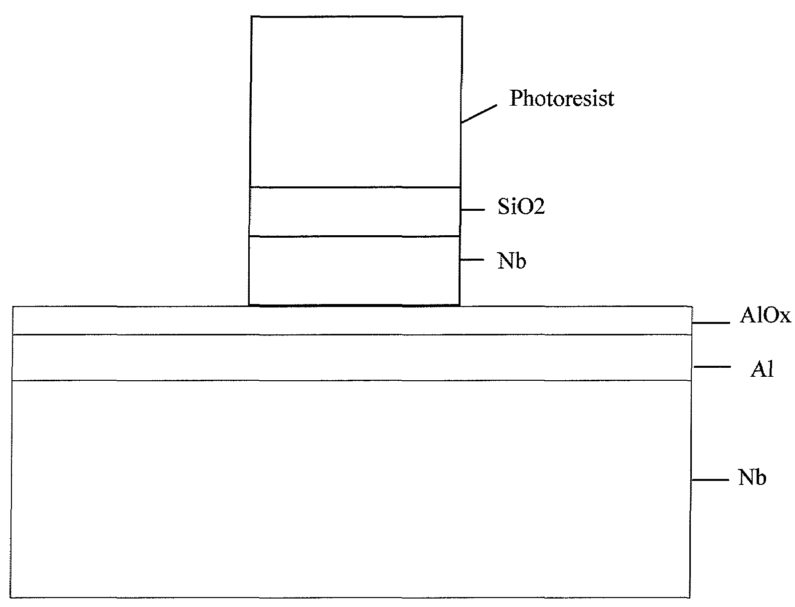
[0034]A new fabrication method is proposed for increasing the yield and quality of superconducting junctions and more particularly Josephson junctions and Josephson-based digital and analog circuits in superconducting electronics. The method is based on using a double-layer mask for partial anodization of the junction side-walls and base-electrode around the junction. The top layer of this mask is a photoresist or electron-beam resist, and the bottom layer is a dielectric (e.g., SiO2) that is insoluble in either aqueous or organic solvents. A more detailed description will now be given.

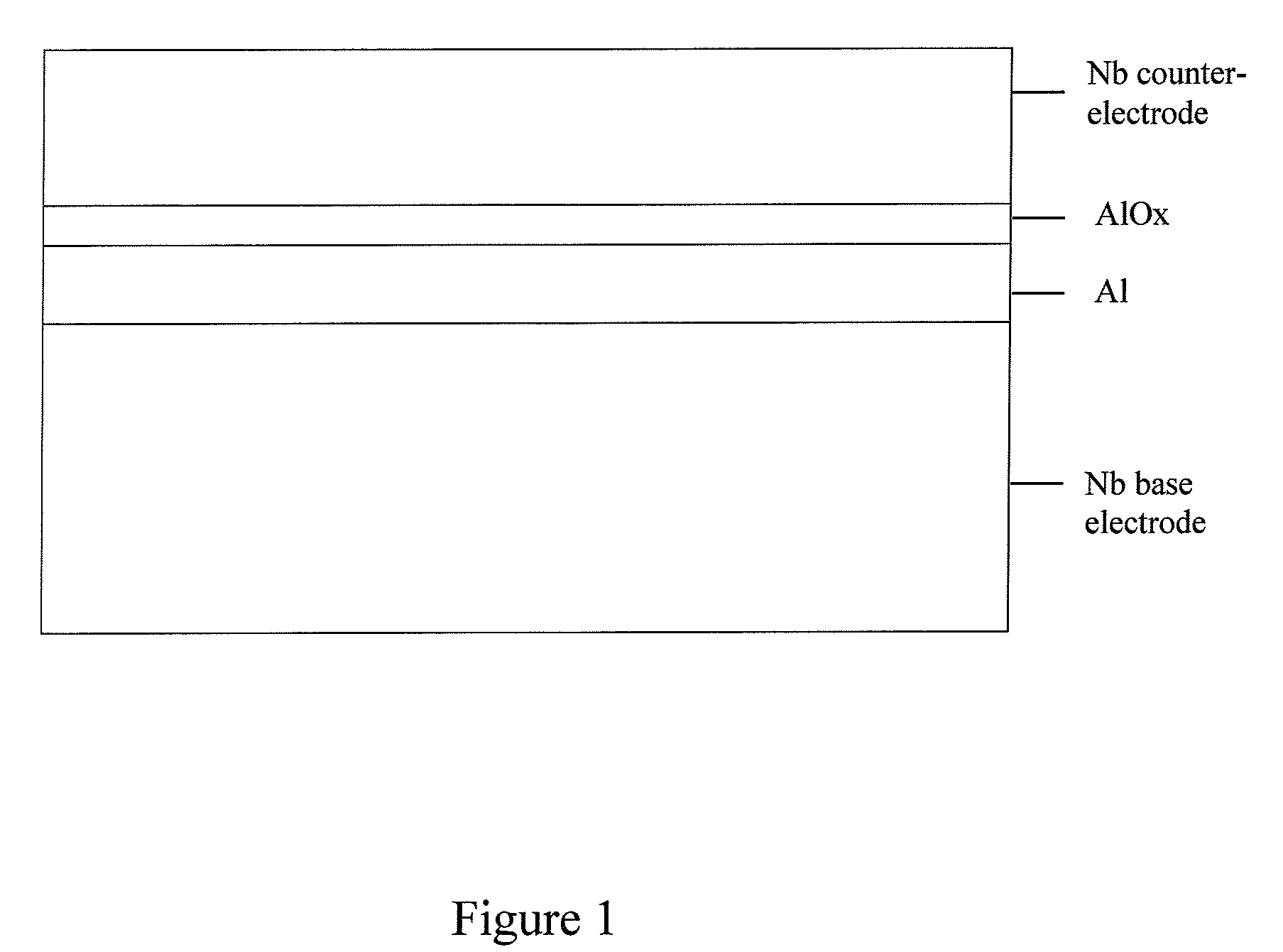
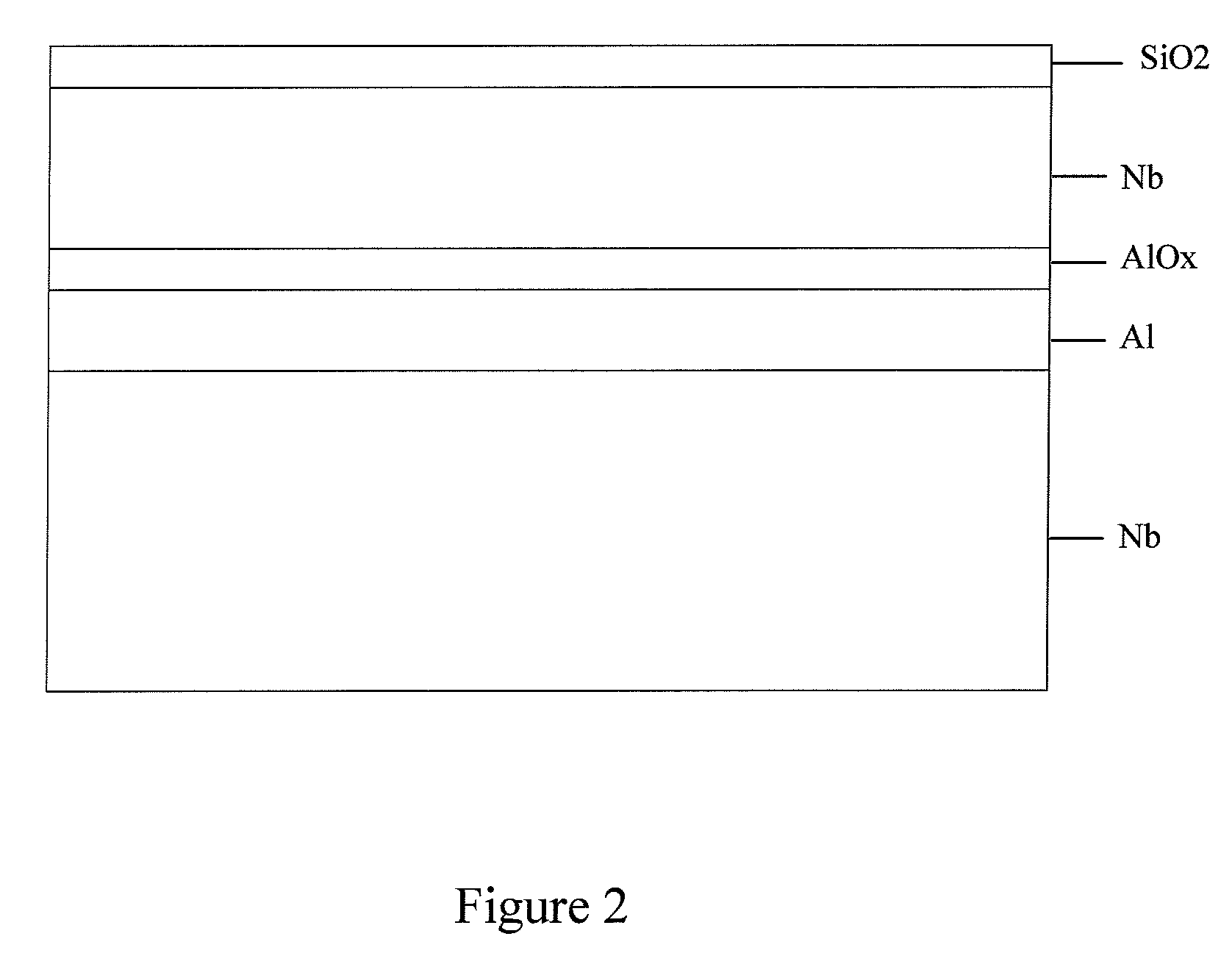
[0035]The existing fabrication scheme for making Nb-based Josephson tunnel junctions for superconducting electronics is comprised of the following fabrication steps:[0036]1. As shown in FIG. 1, a Nb / Al / AlOx / Nb trilayer is deposited in-situ on a wafer that includes or will include several other patterned layers of metal and dielectric. A tunnel barrier is formed by in-situ thermal oxidation of the Al l...


PUM


Abstract

A new technique is presented for improving the microfabrication yield of Josephson junctions in superconducting integrated circuits. This is based on the use of a double-layer lithographic mask for partial anodization of the side-walls and base electrode of the junctions. The top layer of the mask is a resist material, and the bottom layer is a dielectric material chosen so as to a) maximize adhesion between the resist and the underlying superconducting layer, b) be etch-compatible with the underlying superconducting layer, and c) be insoluble in the resist and anodization processing chemistries. In a preferred embodiment of the invention, the superconductor is niobium, the material on top of this is silicon dioxide, and the top layer is conventional photoresist or electron-beam resist. The use of this combination results in a substantial increase in the fabrication yield of high-density superconducting integrated circuits due to increase in junction uniformity and reduction in defect density. An additional improvement over the prior art involves the replacement of a wet-etch step with a dry etch more compatible with microlithography.

Description

CROSS REFERENCE TO RELATED APPLICATIONS[0001]This application is related to and claims priority to Provisional Application 60 / 826,262 filed Sep. 20, 2006 by inventor Sergey K. Tolpygo entitled A Double-Masking Technique for Increasing Fabrication Yield and Josephson Junction Quality in Superconducting Electronics, the contents of which are incorporated herein by reference in its entirety.[0002]This invention was developed in part under contract number N0014-03-C-0370 from the Office of Naval Research, Deborah Van Vechten, Contract Administrator.BACKGROUND OF THE INVENTION[0003]1. Field of the Invention[0004]The invention is directed to fabrication of electronic devices and more particularly to the fabrication of superconducting electronic devices such as Josephson junctions.[0005]2. Description of the Prior Art[0006]Superconducting integrated circuits (ICs) based on Josephson junctions offer the possibility of operation at clock frequencies of 100 GHz or above. In order to achieve t...

Claims


Application Information

Patent Timeline
Patent Type & Authority Patents(United States)
IPC IPC(8): H01L21/00
CPCH01L39/025H01L39/2493H10N69/00H10N60/12H10N60/0912H10N60/85H10N60/0156H10N60/805H10N60/0884
Inventor TOLPYGO, SERGEY K.
Owner SEEQC INC
Why Eureka
Try Eureka