Semiconductor die package including multiple dies and a common node structure

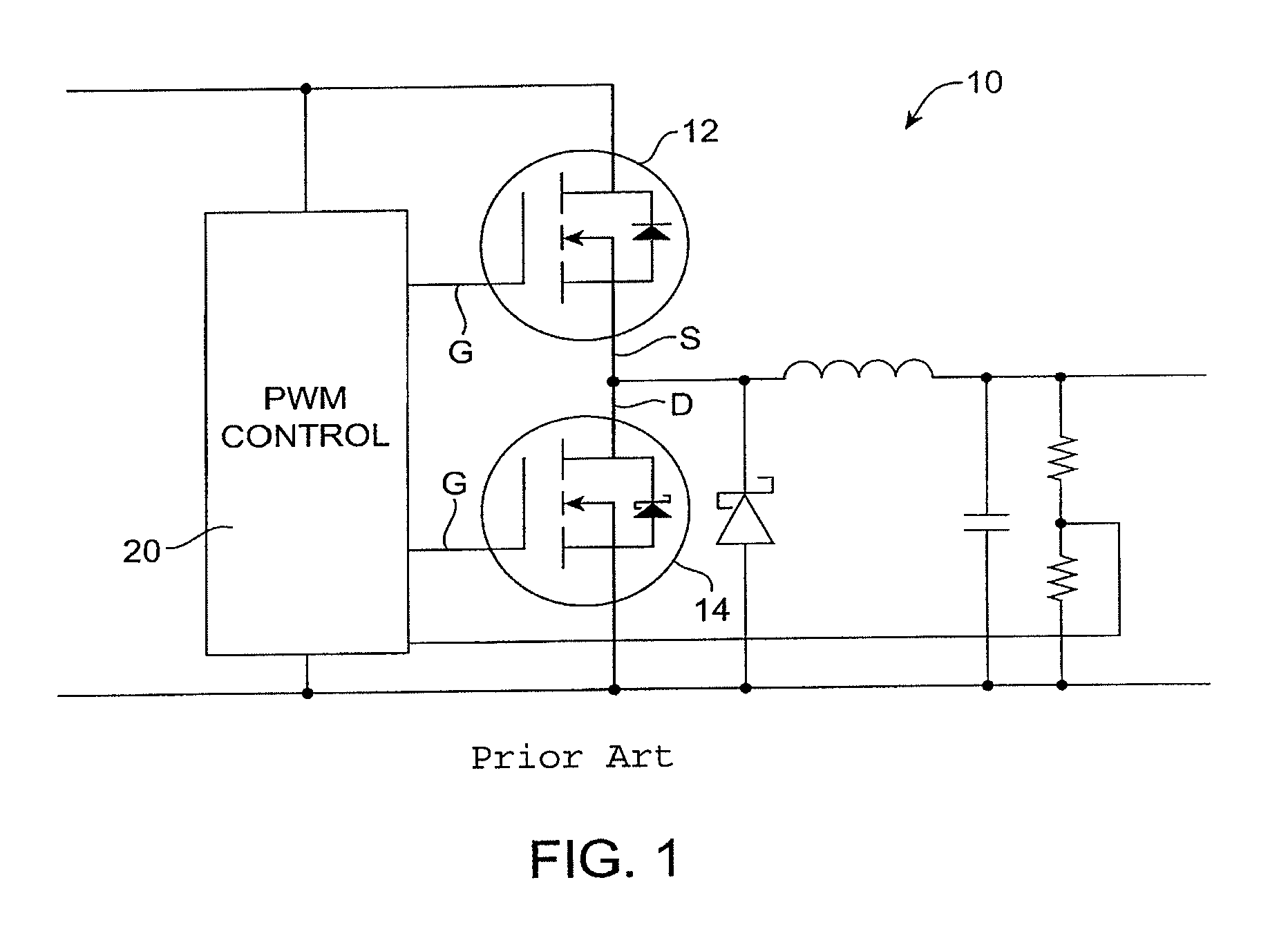
a technology of micro-conductor and die, applied in the direction of semiconductor devices, semiconductor/solid-state device details, electrical apparatus, etc., can solve the problems of reducing the high-frequency power efficiency and thermal performance of conventional packages, high parasitic inductance, and not being well-suited to carrying moderate to high current levels

Active Publication Date: 2009-11-17
SEMICON COMPONENTS IND LLC
View PDF68 Cites 37 Cited by
  • Summary
  • Abstract
  • Description
  • Claims
  • Application Information

AI Technical Summary

Benefits of technology

[0054]Embodiments of the invention have a number of advantages. First, referring to FIG. 2(a), in embodiments of the invention, cooling can occur from the top of the package 100 through the switch node clip 52 and from the bottom through the leadframe structure 51. Second, in embodiments of the invention, the switch node connection (switch node clip 52) is contained in the package and does not rely on a motherboard. Third, a controller die, a high side MOSFET and a low side MOSFET may be contained in a single package thereby providing for a compact component for a synchronous buck converter. Fourth, since the switch node is inside of the package, this minimizes the loop length for connection between the high side source and the low side drain, thus reducing parasitic inductance in the power path. There are also fewer wirebonds thereby reducing the package's inductance and resistance. All of these characteristics allow for higher switching frequencies and higher power density. Fifth, the formed package may have a micro-leadframe (MLP) type configuration and can be mounted to a motherboard in a conventional manner. Special mounting processes are not needed.

Problems solved by technology

Such fully integrated devices, however, tend to be fairly application and / or design specific devices that are often not compatible with other applications and / or designs.
Further, the printed circuit board traces / conductors that connect the MOSFETs are typically not well-suited to carrying moderate to high levels of current.
This creates high parasitic inductance.
Such factors reduce the high-frequency power efficiency and thermal performance of conventional packages.
Moreover, in general, multi die paddle devices are laterally arranged as a result of which the physical size of the package is larger leading to lower package reliability (e.g. sensitivity to moisture during reflow / soldering / mounting processes).

Method used


Image

  • Semiconductor die package including multiple dies and a common node structure
  • Semiconductor die package including multiple dies and a common node structure
  • Semiconductor die package including multiple dies and a common node structure

Examples


Embodiment Construction

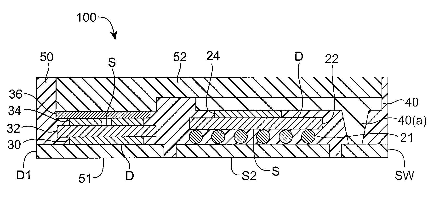
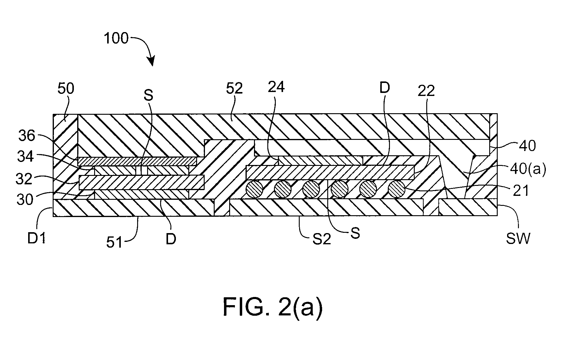
[0021]Embodiments of the invention are directed to semiconductor die packages and methods for making semiconductor die packages. A semiconductor die package according to an embodiment of the invention comprises a substrate, and a first semiconductor die mounted on the substrate, where the first semiconductor die comprises a first vertical device (e.g., a low side MOSFET) comprising a first input region (e.g., a source region) and a first output region (e.g., a drain region) at opposite surfaces of the first semiconductor die. The semiconductor die package comprises a second semiconductor die mounted on the substrate. The second semiconductor die comprises a second vertical device (e.g., a high side MOSFET) comprising a second input region (e.g., a source region) and a second output region (e.g., a drain region) at opposite surfaces of the second semiconductor die. A conductive node clip electrically communicates the first output region in the first semiconductor die and the second i...


PUM


Abstract

A semiconductor die package capable of being mounted to a motherboard is disclosed. The semiconductor die package includes a substrate, and a first semiconductor die mounted on the substrate, where the first semiconductor die includes a first vertical device comprising a first input region and a first output region at opposite surfaces of the first semiconductor die. The semiconductor die package includes a second semiconductor die mounted on the substrate, where second semiconductor die comprises a second vertical device comprising a second input region and a second output region at opposite surfaces of the second semiconductor die. A substantially planar conductive node clip electrically communicates the first output region in the first semiconductor die and the second input region in the second semiconductor die. The first semiconductor die and the second semiconductor die are between the substrate and the conductive node clip.

Description

CROSS-REFERENCES TO RELATED APPLICATIONS[0001]None.BACKGROUND OF THE INVENTION[0002]Synchronous buck converters are used for voltage regulation. A typical synchronous buck converter can use a controller IC (integrated circuit), a high-side power MOSFET and a low-side power MOSFET.[0003]FIG. 1 shows a simplified circuit diagram of a typical synchronous buck converter. Synchronous buck converter (SBC) 10 includes a high-side metal oxide semiconductor field effect transistor (MOSFET) 12 and a low-side MOSFET 14. The drain D of the low-side MOSFET 14 is electrically connected to the source S of the high-side MOSFET 12, through a node S. A PWM (pulse width modulator) controller can control the gates G of the high and low-side MOSFETs 12, 14.[0004]The node connection between the source S and the drain D of the high and low-side MOSFETs 12 and 14, respectively, in SBC 10, desirably has very low inductance in order for the SBC 10 to be used at moderate to high operating / switching frequencie...

Claims


Application Information

Patent Timeline
Patent Type & Authority Patents(United States)
IPC IPC(8): H01L23/34
CPCH01L23/492H01L23/49524H01L23/49562H01L23/49575H01L24/34H01L2924/1305H01L2924/1306H01L2224/37147H01L2224/73253H01L2924/014H01L2924/01047H01L2924/01024H01L2924/01006H01L2924/01005H01L24/49H01L2224/48137H01L2224/48247H01L2224/49171H01L2924/01013H01L2924/01029H01L2924/01033H01L2924/01046H01L2924/01078H01L2924/01079H01L2924/01082H01L2924/13091H01L2924/14H01L2924/30107H01L24/48H01L2924/00H01L2924/181H01L2224/40245H01L24/40H01L24/37H01L2924/00014H01L2224/84801H01L2224/8385H01L2224/8485H01L24/41H01L2224/83801H01L2224/0603H01L24/84H01L2224/73221H01L2924/00012H01L2224/45099H01L2224/45015H01L2924/207H01L23/48
Inventor JOSHI, RAJEEVIYER, VENKATKLEIN, JONATHAN
Owner SEMICON COMPONENTS IND LLC
Why Eureka
Try Eureka